
Datasheet


www.maximintegrated.com
Maxim Integrated
│
21
MAX11200/MAX11210 24-Bit, Single-Channel, Ultra-Low-Power,
Delta-Sigma ADCs with GPIO
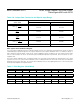
Table 16b. Output Data Formats for the Bipolar Input Range
Table 17. SOC Register (Read/Write)
SOC: System Offset Calibration Register
The system offset calibration register is a 24-bit read/write register. The data written/read to/from this register is clocked
in/out MSB (most significant bit) first. This register holds the system offset calibration value. The format is always in
two’s complement binary format. A write to the system-calibration register is allowed. The value written remains valid
until it is either rewritten or until an on-demand system-calibration operation is performed, which overwrites the user-
supplied value.
The system offset calibration value is subtracted from each conversion result provided the NOSYSO bit in the CTRL3
register is set to 0. The system offset calibration value is subtracted from the conversion result after self-calibration
but before system gain correction. The system offset calibration value is also applied prior to the 1x or 2x scale factor
associated with bipolar and unipolar modes.
BIT B23 B22 B21 B20 B19 B18 B17 B16
DEFAULT
0 0 0 0 0 0 0 0
BIT B15 B14 B13 B12 B11 B10 B9 B8
DEFAULT
0 0 0 0 0 0 0 0
BIT B7 B6 B5 B4 B3 B2 B1 B0
DEFAULT
0 0 0 0 0 0 0 0
INPUT VOLTAGE
V
AINP
- V
AINN
DIGITAL OUTPUT CODE FOR BIPOLAR RANGES
OFFSET BINARY FORMAT TWO’S COMPLEMENT FORMAT
≥ V
REF
0xFFFFFF 0x7FFFFF
0xFFFFFE 0x7FFFFE
0x800001 0x000001
0 0x800000 0x000000
0x7FFFFF 0xFFFFFF
0x000001 0x800001
≤ -V
REF
0x000000 0x800000
REF
23
1
V1
21
×−
−
REF
23
V
21−
REF
23
V
21
−
−
REF
23
1
V1
21
− ×−
−