
Datasheet


www.maximintegrated.com
Maxim Integrated
│
13
MAX11200/MAX11210 24-Bit, Single-Channel, Ultra-Low-Power,
Delta-Sigma ADCs with GPIO
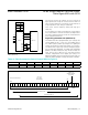
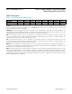
Figure 5. SPI Command Byte
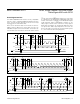
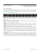
Figure 6. SPI Register Access Write
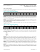
Figure 7. SPI Register Access Read
Serial-Digital Interface
The MAX11200/MAX11210 interface is fully compatible
with SPI-, QSPI-, and MICROWIRE-standard serial inter-
faces. The SPI interface provides access to nine on-chip
registers that are 8 or 24 bits wide.
Drive CS low to transfer data in and out of the devices.
Clock in data at DIN on the rising edge of SCLK. The
RDY/DOUT output serves two functions: conversion sta-
tus and data read. To find the conversion status, assert
CS low and read the RDY/DOUT output; the conversion
is in progress if the RDY/DOUT output reads logic-high
and the conversion is complete if the RDY/DOUT output
reads logic-low. Data at RDY/DOUT changes on the
falling edge of SCLK and is valid on the rising edge of
SCLK. DIN and DOUT are transferred MSB first. Drive
CS high to force DOUT high impedance and cause the
devices to ignore any signals on SCLK and DIN. Figures
5, 6, and 7 show the SPI timing diagrams.
t
CSH0
t
DOE
HIGH-Z
t
DOD
HIGH-Z
t
CSS0
SCLK 0
X
1
10CAL1 CAL0 IMPD RATE2 RATE1 RATE0
8
DIN
t
DH
t
CP
t
CSH1
t
CSS1
t
CSW
t
CL
t
CH
t
DS
CS
RDY/DOUT
t
CSH0
t
DOE
HIGH-Z
t
DOD
HIGH-Z
t
CSS0
SCLK 0
X
1
11X RS3 RS2 RS1 RS0
W/R D7 D6 D5 D4 D3 D2 D1 D0
1689
DIN
t
DH
t
CP
t
CSH1
t
CSS1
t
CSW
t
CL
t
CH
t
DS
CS
RDY/DOUT
t
DOE
HIGH-Z
HIGH-Z
SCLK
X
1
11X RS3 RS2 RS1 RS0
W/R XX X XXXXX
D6D7 D5 D4 D3 D2 D1 D0
1689
DIN
t
CP
t
DOD
t
DOT
t
DO1
t
DOH
CS
RDY/DOUT
t
CSS0
t
DS
t
CSS1
t
CL
t
CH
t
DH