
Datasheet


8 ______________________________________________________________________________________
MAX11208
20-Bit, Single-Channel, Ultra-Low-Power,
Delta-Sigma ADC with 2-Wire Serial Interface
Pin Description
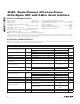
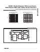
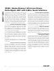
Pin Configuration
1
2
3
4
5
10
9
8
7
6
CLK
SCLK
DVDDAINN
REFN
REFP
GND
MAX11208
µMAX
TOP VIEW
AVDDAINP
RDY/DOUT
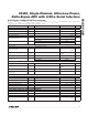
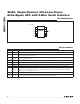
PIN NAME FUNCTION
1 GND Ground. Ground reference for analog and digital circuitry.
2 REFP
Differential Reference Positive Input. REFP must be more positive than REFN. Connect REFP to a
voltage between AVDD and GND.
3 REFN
Differential Reference Negative Input. REFN must be more negative than REFP. Connect REFN to a voltage
between AVDD and GND.
4 AINN Negative Fully Differential Analog Input
5 AINP Positive Fully Differential Analog Input
6 AVDD Analog Supply Voltage. Connect a supply voltage between +2.7V to +3.6V with respect to GND.
7 DVDD Digital Supply Voltage. Connect a digital supply voltage between +1.7V to +3.6V with respect to GND.
8
RDY/DOUT
Data-Ready Output/Serial-Data Output. This output serves a dual function. In addition to the serial-data
output function, the RDY/DOUT also indicates that the data is ready when the RDY is logic-low. RDY/DOUT
changes on the falling edge of SCLK.
9 SCLK Serial-Clock Input. Apply an external serial clock to SCLK.
10 CLK
External Clock Signal Input. The internal clock shuts down when CLK is driven by an external clock. Use a
2.4576MHz oscillator (MAX11208A) or a 2.2528MHz oscillator (MAX11208B).