
Datasheet


21Maxim Integrated
20-Bit, Single-Channel, Ultra-Low-Power, Delta-
Sigma ADCs with Programmable Gain and GPIO
MAX11206/MAX11207
DATA: Data Register
The data register is a 24-bit read-only register. Any attempt to write data to the data register has no effect. The data
read from this register is clocked out MSB first. The data register holds the conversion result. D19 is the MSB, and D0
is the LSB. The result is stored in a format according to the FORMAT bit in the CTRL1 register.
The data format while in unipolar mode is always straight binary. In straight binary format, the most negative value is
0x00000 (V
AINP
- V
AINN
= 0V), the midscale value is 0x80000 (V
AINP
- V
AINN
= V
REF
/2), and the most positive value
is 0xFFFFF (V
AINP
- V
AINN
= V
REF
).
In bipolar mode, if the FORMAT bit = 1, then the data format is offset binary. If the FORMAT bit = 0, then the data
format is two’s complement. In two’s complement the negative full-scale value is 0x80000 (V
AINP
- V
AINN
= -V
REF
), the
midscale is 0x00000 (V
AINP
- V
AINN
= 0V), and the positive full scale is 0x7FFFF (V
AINP
- V
AINN
= V
REF
). Any input
exceeding the available input range is limited to the minimum or maximum data value.
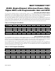
Table 15. DATA Register (Read Only)
Table 16a. Output Data Format for the Unipolar Input Range
BIT D19 D18 D17 D16 D15 D14 D13 D12
DEFAULT
0 0 0 0 0 0 0 0
BIT D11 D10 D9 D8 D7 D6 D5 D4
DEFAULT
0 0 0 0 0 0 0 0
BIT D3 D2 D1 D0
0 0 0 0
DEFAULT
0 0 0 0 0 0 0 0
INPUT VOLTAGE
V
AINP
- V
AINN
DIGITAL OUTPUT CODE FOR UNIPOLAR RANGE
STRAIGHT BINARY FORMAT
≥ V
REF
0xFFFFF
0xFFFFE
0x00001
0 0x00000
REF
20
1
V1
21
×−
−
REF
20
V
21
−