
Datasheet

MAX11190 4-Channel, Dual, Simultaneous Sampling,
2.2V to 3.6V, 12-Bit, 3Msps SAR ADC in Tiny
3mm x 3mm TQFN Package
www.maximintegrated.com
Maxim Integrated
│
6
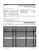
Electrical Characteristics (continued)
(V
DD
= +2.2V to +3.6V, REFA = REFB = V
DD
, OVDD = V
DD
, unless otherwise noted. f
SCLK
= 48MHz, 3Msps, 50% duty cycle.
Reference pins are independent, C
DOUTA/DOUTB
= 10pF. T
A
= -40ºC to 125ºC, unless otherwise noted. Typical values are at
T
A
= +25ºC.) (Note 2)
Note 2: Limitsare100%testedatT
A
=+25°C.Limitsovertheoperatingtemperaturerangeandrelevantsupplyvoltagerangeare
guaranteed by design and characterization, unless otherwise noted.
Note 3: All timing specifications given are with a 10pF capacitor.
Note 4: Guaranteed by design in characterization; not production tested.
PARAMETER SYMBOL CONDITIONS MIN TYP MAX UNITS
POWER SUPPLY
Positive Supply Voltage V
DD
V
DD
pin 2.2 3.6 V
Digital I/O Supply Voltage V
OVDD
OVDD pin 1.5 V
DD
V
Power-Down Current I
PD
Leakageonly,persupplypin 2.6 10 µA
Positive Supply Current
(Full Power Mode)
I
DD
f
SAMPLE
= 3Msps, V
AIN
= 0V, both ADCs 6.8 mA
Positive Supply Current
(Full Power Mode), No Clock
I
DD
f
SAMPLE
= 3Msps, V
DD
= +3V, both ADCs 3.9 mA
LineRejection PSR V
DD
= +2.2V to +3.6V, V
REF
= 2.2V 0.7 LSB/V
TIMING CHARACTERISTICS
Quiet Time t
Q
(Note 4) 4 ns
CS Pulse Width t
1
(Note 4) 10 ns
CSFalltoSCLKSetup t
2
(Note 4) 5 ns
CS Falling until DOUTA/DOUTB
Three-State Disabled
t
3
(Note 4) 1 ns
DataAccessTimeAfterSCLK
Falling Edge
t
4
V
OVDD
= 2.2V to 3.6V 15
ns
V
OVDD
= 1.5V to 2.2V 16.5
SCLKPulse-WidthLow t
5
Percentage of clock period (Note 4) 40 60 %
SCLKPulse-WidthHigh t
6
Percentage of clock period (Note 4) 40 60 %
DataHoldTimefromSCLK
Falling Edge
t
7
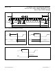
Figure 3 (Note 4) 5 ns
SCLKFallinguntilDOUTA/DOUTB
Three-Stated
t
8
Figure 4 (Note 4) 2.5 14 ns
T-Power Up 1 conversion cycle (Note 4) 1 Cycle