
Datasheet

MAX11190 4-Channel, Dual, Simultaneous Sampling,
2.2V to 3.6V, 12-Bit, 3Msps SAR ADC in Tiny
3mm x 3mm TQFN Package
www.maximintegrated.com
Maxim Integrated
│
5
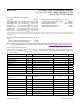
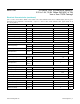
Electrical Characteristics (continued)
(V
DD
= +2.2V to +3.6V, REFA = REFB = V
DD
, OVDD = V
DD
, unless otherwise noted. f
SCLK
= 48MHz, 3Msps, 50% duty cycle.
Reference pins are independent, C
DOUTA/DOUTB
= 10pF. T
A
= -40ºC to 125ºC, unless otherwise noted. Typical values are at
T
A
= +25ºC.) (Note 2)
PARAMETER SYMBOL CONDITIONS MIN TYP MAX UNITS
CONVERSION RATE
Throughput 16 cycles 0.03 3 Msps
Conversion Time 13 cycles 260 ns
Acquisition Time t
ACQ
Track time = 2.5 cycles 52 ns
Aperture Delay From CS falling edge 4 ns
Aperture Delay Matching 150 ps
Aperture Jitter 15 ps
Serial-Clock Frequency f
CLK
0.48 48 MHz
ANALOG INPUT (AIN1A, AIN2A, AIN1B, and AIN2B)
Input Voltage Range
V
INA
AIN1A and AIN2A pins 0 V
REFA
V
V
INB
AIN1B and AIN2B pins 0 V
REFB
V
InputLeakageCurrent I
ILA
0.002 ±1 µA
Input Capacitance C
AIN_
Track 20
pF
Hold 4
EXTERNAL REFERENCE (REFA and REFB)
Input Voltage Range
V
REFA
V
REFB
1 V
DD
+ 0.05 V
InputLeakageCurrent I
ILR
Conversion stopped 0.005 ±1 µA
Input Capacitance
C
REFA
C
REFB
5 pF
DIGITAL INPUTS (SCLK, CS, CHSEL)
Input High Voltage V
IH
0.75 x V
OVDD
V
InputLowVoltage V
IL
0.25 x V
OVDD
V
Input Hysteresis V
HYST
0.15 x V
OVDD
%OVDD/
V
DD
InputLeakageCurrent I
IL
Inputs at 0V or V
OVDD
0.001 ±1 µA
Input Capacitance C
IN
2 pF
DIGITAL OUTPUT (DOUTA and DOUTB)
Output High Voltage V
OH
I
SOURCE
= 1mA 0.85 x V
OVDD
V
OutputLowVoltage V
OL
I
SINK
= 5mA 0.15 x V
OVDD
V
Three-StateLeakageCurrent I
OL
±1.0 µA
Three-State Output Capacitance
(Without Pad Metal)
C
OUT
5 pF