
Datasheet

MAX11190 4-Channel, Dual, Simultaneous Sampling,
2.2V to 3.6V, 12-Bit, 3Msps SAR ADC in Tiny
3mm x 3mm TQFN Package
www.maximintegrated.com
Maxim Integrated
│
4
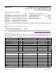
Electrical Characteristics
(V
DD
= +2.2V to +3.6V, REFA = REFB = V
DD
, OVDD = V
DD
, unless otherwise noted. f
SCLK
= 48MHz, 3Msps, 50% duty cycle.
Reference pins are independent, C
DOUTA/DOUTB
= 10pF. T
A
= -40ºC to 125ºC, unless otherwise noted. Typical values are at
T
A
= +25ºC.) (Note 2)
V
DD
to GND ....................................................................... -0.3V to +4V
AIN1A, AIN2A to GND .... -0.3V to the lower of (V
DD
+ 0.3V) and +4.0V
REFA, OVDD to GND ....-0.3V to the lower of (V
DD
+ 0.3V) and +4.0V
AIN1B, AIN2B to GND ....-0.3V to the lower of (V
DD
+ 0.3V) and +4.0V
REFB to GND ................. -0.3V to the lower of (V
DD
+ 0.3V) and +4.0V
CS,SCLKtoGND ..... -0.3V to the lower of (V
OVDD
+ 0.3V) and +4.0V
CHSELtoGND ......... -0.3V to the lower of (V
OVDD
+ 0.3V) and +4.0V
DOUTA to GND
........... -0.3V to the lower of (V
OVDD
+ 0.3V) and +4.0V
DOUTB to GND
.......... -0.3V to the lower of (V
OVDD
+ 0.3V) and +4.0V
Multilayer Board Max Power Dissipation (T
A
= +70ºC)
TQFN (derate 20.8mW/ºC above +70ºC) ..................1667mW
Operating Temperature Range .......................... -40ºC to +125ºC
Storage Temperature Range .............................-65ºC to +150ºC
LeadTemperature(soldering,10s) ................................. +300ºC
Soldering Temperature (reflow) ....................................... +260ºC
Absolute Maximum Ratings
Stresses beyond those listed under “Absolute Maximum Ratings” may cause permanent damage to the device. These are stress ratings only, and functional operation of the device at these
or any other conditions beyond those indicated in the operational sections of the specifications is not implied. Exposure to absolute maximum rating conditions for extended periods may affect
device reliability.
Package Thermal Characteristics
TQFN
Junction-to-AmbientThermalResistance(θ
JA
) ..........48°C/W
Junction-to-CaseThermalResistance(θ
JC
) ...............10°C/W
(Note 1)
Note 1: Package thermal resistances were obtained using the method described in JEDEC specification JESD51-7, using a four-layer
board. For detailed information on package thermal considerations, refer to www.maximintegrated.com/thermal-tutorial.
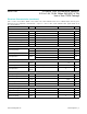
PARAMETER SYMBOL CONDITIONS MIN TYP MAX UNITS
DC ACCURACY
Resolution 12 bit 12 Bits
Integral Nonlinearity INL ±1 LSB
Differential Nonlinearity DNL No missing codes over temperature ±1 LSB
Offset Error ±1 ±4.0 LSB
Gain Error Excluding offset and reference errors ±1 ±4.0 LSB
Total Unadjusted Error TUE ±1.5 LSB
Channel-to-Channel Offset Matching ±0.3 LSB
Channel-to-Channel Gain Matching ±0.3 LSB
DYNAMIC PERFORMANCE
Signal-to-Noise Plus Distortion
(Note 3)
SINAD f
IN
= 1MHz 70 72 dB
Signal-to-Noise Ratio SNR f
IN
= 1MHz 70.5 72 dB
Total Harmonic Distortion THD f
IN
= 1MHz -85 -75 dB
Spurious-Free Dynamic Range SFDR f
IN
= 1MHz 76 85 dB
Intermodulation Distortion IMD f
IN1
= 1.0003MHz, f
IN2
= 0.99955MHz -84 dB
Full-Power Bandwidth -3dB point 40 MHz
Full-LinearBandwidth SINAD > 68dB 2.5 MHz
Small-Signal Bandwidth 45 MHz
Crosstalk Channel to channel -90 dB