
Datasheet

MAX11190 4-Channel, Dual, Simultaneous Sampling,
2.2V to 3.6V, 12-Bit, 3Msps SAR ADC in Tiny
3mm x 3mm TQFN Package
www.maximintegrated.com
Maxim Integrated
│
3
TABLE OF CONTENTS (continued)
LIST OF FIGURES
Full-Power Bandwidth ........................................................................17
Full-LinearBandwidth ........................................................................17
Intermodulation Distortion.....................................................................17
Ordering Information .......................................................................... 18
Chip Information .............................................................................. 18
Package Information .......................................................................... 18
Revision History .............................................................................. 19
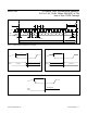
Figure 1. Interface Signals for Maximum Throughput .................................................. 7
Figure2.SetupTimeAfterSCLKFallingEdge ....................................................... 7
Figure3.HoldTimeAfterSCLKFallingEdge ........................................................ 7
Figure4.SCLKFallingEdgeDOUTA/DOUTBThree-State ............................................. 7
Figure 5. Analog Input Circuit ................................................................... 12
Figure 6. Normal Mode ........................................................................ 13
Figure 7. Entering Power-Down Mode ............................................................. 13
Figure 8. Exiting Power-Down Mode .............................................................. 14
Figure 9. ADC Transfer Function ................................................................. 14
Figure 10. Supply Current vs. Sample Rate (Normal Operating Mode) ................................... 14
Figure 11. Supply Current vs. Sample Rate (Device Powered Down Between Conversions) .................. 14
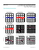
Figure 12. Channel Select Timing Diagram ......................................................... 15
Figure 13. 14-Clock Cycle Operation.............................................................. 15
Figure 14. Typical Application Circuit.............................................................. 16