
Datasheet


MAX11190 4-Channel, Dual, Simultaneous Sampling,
2.2V to 3.6V, 12-Bit, 3Msps SAR ADC in Tiny
3mm x 3mm TQFN Package
www.maximintegrated.com
Maxim Integrated
│
14
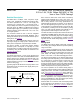
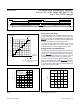
Figure 9. ADC Transfer Function
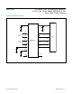
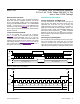
Figure 8. Exiting Power-Down Mode
Exiting Power-Down Mode
To exit power-down mode, implement one dummy conver-
sion by driving CS low for at least 10 clock cycles (see
Figure 8). The data on DOUTA/DOUTB is invalid during
this dummy conversion. The first conversion following the
dummy cycle contains a valid conversion result.
The power-up time equals the duration of the dummy
cycle, and is dependent on the clock frequency. The
power-uptimeforthisdevice(48MHzSCLK)is333ns.
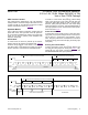
Supply Current vs. Sampling Rate
For applications requiring lower throughput rates, the user
can reduce the clock frequency (f
SCLK
) to lower the sam-
ple rate. Figure 10 shows the typical supply current (I
VDD
)
as a function of sample rate (f
S
) for the device. The part
operates in normal mode and is never powered down.
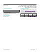
The user can also power down the ADC between conver-
sions by using power-down mode. Figure 11 shows this
device as the sample rate is reduced, the device remains
in the power-down state longer and the average supply
current (I
VDD
) drops accordingly.
Figure 10. Supply Current vs. Sample Rate (Normal Operating
Mode)
Figure 11. Supply Current vs. Sample Rate (Device Powered
Down Between Conversions)
123456789
10 11 12 13 14 15 16
N12345678910 11 12 13 14 15 16
HIGH
IMPEDANCE
HIGH
IMPEDANCE
HIGH
IMPEDANCE
SCLK
CS
DOUTA
DOUTB
INVALID DATA (DUMMY CONVERSION) VALID DATA
FS - 1.5 x LSB
OUTPUT CODE
ANALOG
INPUT (LSB)
111...111
111...110
111...101
0 123 2
n
-2 2
n
-1 2
n
000...000
000...001
000...010
FULL SCALE (FS):
AIN1A/AIN1B/AIN2A/AIN2B = REFA/REFB
n = RESOLUTION
f
S
(ksps)
I
VDD
(mA)
2000 25001000 1500
1
2
3
4
5
6
7
8
9
10
0
0 3000
V
DD
= 3V
f
SCLK
= VARIABLE
16 CYCLES/CONVERSION
500
f
S
(ksps)
I
VDD
(mA)
800600400200
1
2
3
4
5
6
0
0 1000
V
DD
= 3V
f
SCLK
= 48MHz