
Datasheet


MAX11190 4-Channel, Dual, Simultaneous Sampling,
2.2V to 3.6V, 12-Bit, 3Msps SAR ADC in Tiny
3mm x 3mm TQFN Package
www.maximintegrated.com
Maxim Integrated
│
12
Detailed Description
The MAX11190 is a 3Msps, 12-bit, low-power, single-
supply, dual, multiplexed simultaneous-sampling ADC.
The device operates from a 2.2V to 3.6V supply and
consumes only 16.4mW (V
DD
= 3V)/10.5mW (V
DD
=
2.2V) at 3Msps. This device is capable of sampling at full
rate when driven by 48MHz. The MAX11190 provides a
separate digital supply input (OVDD) to power the digital
interface enabling communication with 1.5V, 1.8V, 2.5V,
or 3V digital systems.
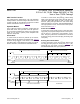
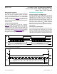
The conversion results for each of the two integrated
ADCs appear at DOUTA and DOUTB, MSB first, with a
leading zero followed by the 12-bit results followed by two
trailing zeros. See Figure 1.
Each ADC core has an independent reference input. The
input signal range for analog inputs is defined as 0V to
V
REF
(V
REF
of respective core) with respect to GND.
This device includes a power-down feature allowing
minimized power consumption at 5µA/ksps for lower
throughput rates. The wake-up and power-down feature is
controlled by using the SPI interface as described in the
Operation Modes section.
Serial Interface
The MAX11190 features a 3-wire serial interface that
directly connects to SPI, QSPI, and MICROWIRE devices
without external logic—DOUTA and DOUTB need to be
received by the host at the same time. Figure 1 shows the
interface signals for a single conversion frame to achieve
maximum throughput.
The falling edge of CS defines the sampling instant. Once
CStransitionslow,theexternalclocksignal(SCLK)con-
trols the conversion.
Each of the two SAR cores of this device successively
extracts binary-weighted bits in every clock cycle. The
MSB appears on the data bus during the 2nd clock cycle
with a delay outlined in the timing specifications. All
extracted data bits appear successively on the data bus
with the LSB appearing during the 13th clock cycle for
12-bit operation. The serial data stream of conversion bits
is preceded by a leading zero and succeeded by trailing
zeros. The data outputs (DOUTA and DOUTB) go into
high-impedance state during the 16th clock cycle.
To sustain the maximum sample rate, all devices have to be
resampled immediately after the 16th clock cycle. For lower
sample rates, the CS falling edge can be delayed leaving
DOUTA/DOUTB in a high-impedance condition. Pull CS
highafterthe10thSCLKfallingedge(seetheOperation
Modes section).
Analog Input
The MAX11190 produces digital outputs that correspond
to the analog input voltages within the specified operating
range of 0 to V
REF
.
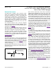
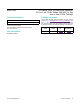
Figure 5 shows an equivalent circuit for the analog input
AIN1A/AIN1B/AIN2A/AIN2B. Internal protection diodes D1/
D2 confine the analog input voltage within the power rails
(V
DD
, GND). The analog input voltage can swing from
V
GND
- 0.3V to V
DD
+ 0.3V without damaging the device.
The electric load presented to the external stage driving
the analog input varies depending on which mode the ADC
is in: track mode vs. conversion mode. In track mode, the
internal sampling capacitor, C
S
(16pF), must be charged
throughtheresistor,R(50Ω),totheinputvoltage.Forfaith-
ful sampling of the input, the capacitor voltage on CS has to
settle to the required accuracy during the track time.
The source impedance of the external driving stage in
conjunction with the sampling switch resistance affects the
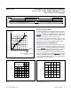
settling performance. The THD vs. Input Resistance graph
in the Typical Operating Characteristics shows THD sensi-
tivityasafunctionofthesignalsourceimpedance.Keep
the source impedance at a minimum for high-dynamic per-
formance applications. Use a high-performance op amp,
such as the MAX4430, to drive the analog input, thereby
decoupling the signal source and the ADC.
While the ADC is in conversion mode, the sampling switch
is open presenting a pin capacitance, C
P
(C
P
= 5pF), to the
driving stage. See the Applications Information section for
information on choosing an appropriate buffer for the ADC.
Figure 5. Analog Input Circuit
C
P
A
IN1A/AIN1B/
A
IN2A/AIN2B
V
DD
A
IN
D2
D1
R
C
S
SWITCH CLOSED IN TRACK MODE
SWITCH OPEN IN CONVERSION MODE