
Datasheet

MAX11190 4-Channel, Dual, Simultaneous Sampling,
2.2V to 3.6V, 12-Bit, 3Msps SAR ADC in Tiny
3mm x 3mm TQFN Package
www.maximintegrated.com
Maxim Integrated
│
10
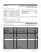
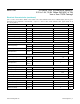
Pin Description
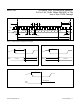
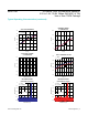
Pin Conguration
PIN NAME FUNCTION
1 DOUTA Serial-DataOutputofADCA.DOUTAchangesstateonSCLK’sfallingedge.
2 DOUTB Serial-DataOutputofADCB.DOUTBchangesstateonSCLK’sfallingedge.
3 SCLK Serial-ClockInput.SCLKdrivestheconversionprocessandclocksdataout.
4 GND Ground. This pin must connect to a solid ground plane.
5 AIN1A Channel 1 of ADC A
6 AIN1B Channel 1 of ADC B
7 AIN2A Channel 2 of ADC A
8 AIN2B Channel 2 of ADC B
9 REFA Reference Pin for ADC A
10 REFB Reference Pin for ADC B
11, 12 V
DD
Positive Supply Voltage
13 GND Ground. This pin must connect to a solid ground plane.
14 CS ChipSelect(Active-Low).Initiatespower-upandacquisitiononthefallingedge.
15 CHSEL
ChannelSelectPinReferringtoAIN1A/AIN1BandAIN2A/AIN2B.SetCHSELlowtoselectAIN1A/
AIN1B for conversion.
16 OVDD
Digital I/O Supply Voltage (CS,CHSEL,DOUTA,DOUTB,SCLK).BypasstoGNDwitha
4.7µF ceramic capacitor.
— EP Exposed pad, internally connected to ground. Connect to a solid ground plane.
15
16
14
13
5
6
7
SCLK
GND
8
DOUTA
REFB
REFA
V
DD
13
CS
EP*
*EP = EXPOSED PAD.
4
12 10 9
CHSEL
OVDD
AIN2B
AIN2
A
AIN1B
AIN1
A
DOUT
BV
DD
2
11
GND
TQFN
MAX11190
TOP VIEW
+