
Datasheet

���������������������������������������������������������������� Maxim Integrated Products 11
MAX11101
14-Bit, +5V, 200ksps ADC with 10µA Shutdown
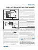
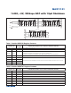
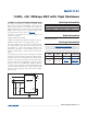
A CS falling edge initiates an acquisition sequence. The
analog input is stored in the capacitive DAC, DOUT
changes from high impedance to logic-low, and the ADC
begins to convert after the sixth clock cycle. SCLK drives
the conversion process and shifts out the conversion
result on DOUT.
SCLK begins shifting out the data (MSB first) after the fall-
ing edge of the 8th SCLK pulse. Twenty-four falling clock
edges are needed to shift out the eight leading zeros, 14
data bits, and 2 sub-bits (S1 and S0). Extra clock pulses
occurring after the conversion result has been clocked
out, and prior to the rising edge of CS, produce trail-
ing zeros at DOUT and have no effect on the converter
operation.
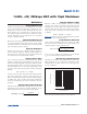
Force CS high after reading the conversion’s LSB to
reset the internal registers and place the MAX11101 in
shutdown. For maximum throughput, force CS low again
to initiate the next conversion immediately after the speci-
fied minimum time (t
CSW
).
Note: Forcing CS high in the middle of a conversion
immediately aborts the conversion and places the
MAX11101 in shutdown.
Figure 6. External Timing Diagram
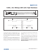
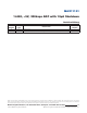
Figure 7. Shutdown Sequence
CS
SCLK
2016
24
1214 86
DOUT
D13 D12 D11
D10 D9 D8 D7
S1 S0D6 D3 D2 D1 D0D5 D4
t
CSH
t
TR
t
DO
t
ACQ
t
CSS
t
CH
t
CL
t
DN
COMPLETE CONVERSION SEQUENCE
CONVERSION 0
CONVERSION 1
POWERED UPPOWERED UP POWERED DOWN
DOUT
CS