
Datasheet


MAX1106/MAX1107
Single-Supply, Low-Power,
Serial 8-Bit ADCs
______________________________________________________________________________________ 15
Layout, Grounding, and Bypassing
For best performance, use printed circuit boards. Wire-
wrap boards are not recommended. Board layout
should ensure that digital and analog signal lines are
separated from each other. Do not run analog and digi-
tal (especially clock) lines parallel to one another or run
digital lines underneath the ADC package.
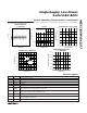
Figure 10 shows the recommended system-ground
connections. A single-point analog ground (star-ground
point) should be established at the A/D ground.
Connect all analog grounds to the star ground. No digi-
tal-system ground should be connected to this point.
The ground return to the power supply for the star
ground should be low impedance and as short as pos-
sible for noise-free operation.
High-frequency noise in the V
DD
power supply may
affect the comparator in the ADC. Bypass the supply to
the star ground with 0.1µF and 1µF capacitors close to
the V
DD
pin of the MAX1106/MAX1107. Minimize
capacitor lead lengths for best supply-noise rejection. If
the power supply is very noisy, a 10Ω resistor can be
connected to form a lowpass filter.
GND
+3V/+5V
SYSTEM POWER SUPPLIES
V
DD
DGNDV
DD
IN-
1µF
10Ω
0.1µF
GND
DIGITAL
CIRCUITRY
MAX1106
MAX1107
Figure 10. Power-Supply Connections
Chip Information
TRANSISTOR COUNT: 2373