
Datasheet


MAX1106/MAX1107
Single-Supply, Low-Power,
Serial 8-Bit ADCs
14 ______________________________________________________________________________________
When operating at speeds below the maximum sam-
pling rate, the MAX1106/MAX1107’s power-down mode
can save considerable power by placing the converter
in a low-current shutdown state between conversions.
Pull SHDN low after the conversion byte has been read
to shut down the device completely.
CONVST should remain low most of the time and tog-
gled high for 1µs (100µs max) for the autozero adjust-
ment. An external reference is recommended for best
accuracy when using the shutdown feature. This
requires only 20µs for the internal biasing circuit to sta-
bilize before starting a new conversion. Alternatively,
the internal reference can be used, but additional time
is required for the reference to stabilize (when
bypassed by a 1µF capacitor; at data rates above
1ksps, the reference stabilizes within 1LSB in 200µs). If
the reference is completely discharged it requires
12ms to settle. No conversions should be performed
until the reference voltage has stabilized.
Internal or External Voltage Reference
An external reference between 1V and V
DD
should be
connected directly at the REFIN pin. To use the internal
reference, connect REFOUT directly to REFIN and
bypass REFOUT with a 1µF capacitor. The DC input
impedance at REFIN is extremely high, consisting of
leakage current only (typically 10nA). During a conver-
sion, the reference must be able to deliver up to 20µA
average load current and have an output impedance of
1kΩ or less at the conversion clock frequency. If the
reference has higher output impedance or is noisy,
bypass it close to the REFIN pin with a 0.1µF capacitor.
The internal reference is active as long as SHDN is high
and powers down when SHDN is low.
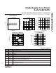
Transfer Function
Figure 9 depicts the input/output transfer function.
Code transitions occur at integer LSB values. Output
coding is binary; with a 2.048V reference 1LSB = 8mV
(V
REFIN
/ 256). For single-ended operation connect IN-
to GND. Full-scale is achieved at V
IN+
= V
REFIN
- 1LSB.
For pseudo-differential operation the V
IN-
voltage range
is from GND to V
DD
, where full-scale is achieved at
V
IN+
= V
REFIN
+ V
IN-
- 1LSB. V
IN+
should not be higher
than V
DD
+ 50mV. Negative input voltages are invalid
and give a zero output code. Voltages greater than full-
scale give an all ones output code.
OUTPUT CODE
FULL-SCALE
TRANSITION
11111111
11111110
11111101
00000011
00000010
00000001
00000000
123
0
FS
FS - 1LSB
FS = V
REFIN
+ V
IN-
1LSB = V
REFIN
256
INPUT VOLTAGE (LSB)
(IN-)
Figure 9. Input/Output Transfer Function