
Datasheet


MAX1106/MAX1107
Single-Supply, Low-Power,
Serial 8-Bit ADCs
10 ______________________________________________________________________________________
_______________Detailed Description
The MAX1106/MAX1107 analog-to-digital converters
(ADCs) use a successive-approximation conversion
technique and input track/hold (T/H) circuitry to convert
an analog signal to an 8-bit digital output. A simple ser-
ial interface provides easy interface to microprocessors
(µPs). No external hold capacitors are required. All of
the MAX1106/MAX1107 operating modes are pin con-
figurable: internal or external reference, single-ended
or pseudo-differential unipolar conversion, and power
down. Figure 3 shows the typical operating circuit.
Analog Inputs
Track/Hold
The input architecture of the ADCs is illustrated in
Figure 4’s equivalent-input circuit of and is composed
of the T/H, the input multiplexer, the input comparator,
the switched capacitor DAC, and the auto-zero rail.
The device is in acquisition mode most of the time.
During the acquisition interval, the positive input (IN+)
is tracked and is connected to the holding capacitor
(C
HOLD
). The acquisition interval ends with the falling
edge of CONVST. At this point the T/H switch opens
and C
HOLD
is connected to the negative input (IN-),
retaining charge on C
HOLD
as a sample of the signal at
IN+. Once conversion is complete the T/H returns
immediately to its tracking mode.
The time required for the T/H to acquire an input signal
is a function of how quickly its input capacitance is
charged. If the input signal’s source impedance is high,
the acquisition time lengthens, and more time must be
allowed between conversions. The acquisition time,
t
ACQ
, is the minimum time needed for the signal to be
acquired. It is calculated by:
t
ACQ
= 6(R
S
+ R
IN
)18pF
VDD
3k
C
LOAD
GND
DOUT
C
LOAD
GND
3k
DOUT
a) V
OL
to V
OH
b) High-Z to V
OL
and V
OH
to V
OL
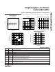
Figure 1. Load Circuits for Enable Time
V
DD
3k
C
LOAD
GND
DOUT
C
LOAD
GND
3k
DOUT
a) V
OH
to High-Z b) V
OL
to High-Z
Figure 2. Load Circuits for Disable Time
V
DD
I/O
SCK (SK)
MISO (SI)
GND
DOUT
SCLK
CONVST
GND
SHDN
V
DD
IN-
1µF
0.1µF
1µF
ON
OFF
IN+
ANALOG
INPUTS
MAX1106
MAX1107
CPU
V
DD
REFOUT
REFIN
Figure 3. Typical Operating Circuit
IN-
IN+
REFIN
GND
C
HOLD
CAPACITIVE DAC
COMPARATOR
18pF
R
IN
6.5k
AUTOZERO
RAIL
TRACK
HOLD
Figure 4. Equivalent Input Circuit