
Datasheet


Belden 8451 works well for distances up to 100 feet in a
noisy environment. Connect the shield to SH0-0H.
Cable resistances affect remote-sensor accuracy; 1Ω
series resistance introduces +0.45°C error.
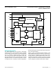
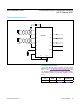
Remote Diode Shielding
Temperature measurements will reflect significant error if
a portion of the bias current supplied to the diode anode
is allowed to flow through parallel paths to ground. If the
diode-connected transistor is mounted on a PCB, sup-
press error-producing “leakage” current by surrounding
the collector/base leads with a metal trace that is con-
nected to the SHO shield output (Figure 8).
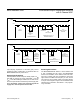
Layout, Grounding, and Bypassing
For best performance, use PCBs. Do not use wirewrap
boards. Board layout should ensure that digital and ana-
log signal lines are separated from each other. Do not run
analog and digital (especially clock) signals parallel to one
another or run digital lines underneath the ADC package.
High-frequency noise in the V
DD
power supply may affect
ADC performance. Bypass the supply with a 0.1μF capac-
itor close to pin V
DD
. Minimize capacitor lead lengths for
best supply-noise rejection. If the power supply is very
noisy, connect a 10Ω resistor in series with the supply to
provide lowpass filtering.
Denitions
Relative Accuracy
Relative accuracy is the deviation of the values on an
actual transfer function from a straight line. This straight
line can be either a best-straight-line fit or a line drawn
between the endpoints of the transfer function, once offset
and gain errors have been nullified. The static linearity
parameters for the MAX1098/MAX1099 are measured
using the best-straight-line fit method.
Differential Nonlinearity (DNL)
Differential nonlinearity is the difference between an actu-
al step width and the ideal value of 1 LSB. A DNL error
specification of less than 1 LSB guarantees no missing
codes and a monotonic transfer function.
Offset Error
Offset error is the difference between the ideal and the
actual offset points. For an ADC, the offset point is the
midstep value when the digital output is zero.
Gain Error
Gain or full-scale error is the difference between the ideal
and actual gain points on the transfer function, after the
offset error has been canceled out. For an ADC, the gain
point is the midstep value when the digital output is full
scale.
Aperture Delay
Aperture delay (t
AD
) is the time defined between the rising
edge of the sampling clock and the instant when an actual
sample is taken.
Figure 8. Remote Diode Shielding for PC Boards
ANODE
SHIELD
CATHODE
MAX1098/MAX1099 10-Bit Serial-Output Temperature Sensors
with 5-Channel ADC
www.maximintegrated.com
Maxim Integrated
│
18
Chip Information
PROCESS: BiCMOS