
Datasheet


the power requirement of an internal reference buffer ampli-
fier that can accommodate external loads. Temperature
conversions at 100% duty cycle increase supply currents
to 440μA (400μA) through additional amplification, buffer,
and bias circuitry that is otherwise inactive.
Place the MAX1098/MAX1099 in a low-current power-
down state between conversions to conserve power.
Select standby, standby plus, or shutdown through bits
PM1 and PM0 of the initialization byte (Table 3).
The MAX1098/MAX1099 assume the shutdown power
mode when V
DD
is first applied.
Standby Mode
Standby mode turns off the MAX1098/MAX1099 ADC,
internal clock, and reference buffer amplifier. Special
circuitry for temperature conversions is also deactivated.
Wake-up time is limited by the reference buffer ampli-
fier and the associated bypass capacitor (see Internal
Reference). When an external reference is used, wake-up
time is 0.1ms.
Standby-Plus Mode
Standby-plus mode is similar to the standby mode, but the
internal reference output buffer remains active to shorten
the wake-up time to 0.1ms for internal reference mode.
When using an external reference, standby-plus mode is
equivalent to standby mode.
Shutdown Mode
Shutdown mode turns off all functions other than startup
circuitry, thereby reducing typical supply current to 2μA.
Data registers are cleared. Use this power mode when
interconversion times are no less than 5ms.
Monitoring V
DD
This mode of operation samples and converts the supply
voltage, V
DD
/4, which is internally generated. The refer-
ence voltage must be larger than V
DD
/8 for the operation
to work properly. From the result of a conversion (CODE),
CODE = 64 V
DD
/V
REF
.
Temperature Measurements
The MAX1098/MAX1099 perform temperature measure-
ments with internal or external diode-connected transis-
tors through a three-step process. First, the diode bias
current changes from 31.6μA to 10μA to produce a
temperature-dependent bias voltage difference, which is
amplified by a factor of 20 and converted to digital format.
Second, the bias current changes from 31.6μA to 100μA,
and the bias voltage difference is similarly amplified by
a factor of 20 and converted to digital format. Third, the
intermediate results are subtracted to achieve a digital
output that is proportional to absolute temperature in
degrees Kelvin.
The reference voltage used in conjunction with tempera-
ture measurements is derived from the internal reference
source to ensure that 1 LSB corresponds to 1/8 of a
degree. To convert to degrees Celsius, subtract 273.15
from the temperature inferred from the ADC output.
Temperature measurements require a conversion time of
2.2ms.
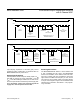
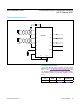
Shield Output Buffer
The MAX1098/MAX1099 provide a shield output buffer
voltage at SHO that is approximately 0.6V (one diode
drop) above V
DD
/2. When performing temperature mea-
surements with an external diode, use this voltage to
suppress error-producing leakage currents (see Remote
Diode Shielding). Figure 7 shows the SHO output circuit.
Applications Information
Remote Diode Selection
Temperature accuracy depends on having a good-quality,
diode-connected, small-signal transistor. Accuracy has
been experimentally verified for 2N3904 devices. CPUs
and other ICs having on-board temperature-sensing
diodes can also be monitored if the diode connections
are uncommitted.
See Power Requirements in Electrical Characteristics.
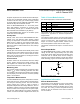
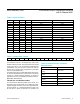
Table 3. Power-Mode Selection
Figure 7. SHO Output Circuit
PM1 PM0 MODE
0 0 Shutdown
0 1 Standby plus
1 0 Standby
1 1 Normal operation
5µA
SHO
V
DD
2
MAX1098/MAX1099 10-Bit Serial-Output Temperature Sensors
with 5-Channel ADC
www.maximintegrated.com
Maxim Integrated
│
16