
Datasheet


input sampling capacitance of the ADC (4pF). Source
impedances below 100kΩ have no significant effect on
MAX1098/MAX1099 AC performance.
Analog Input Protection
Internal protection diodes clamp the analog inputs to V
DD
and GND so channels can swing within GND - 0.3V and
V
DD
+ 0.3V without damage. However, for accurate conver-
sions, the inputs should not extend beyond the supply rails.
If an off-channel analog input extends beyond the
supply rails, limit the input current to 2mA.
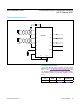
Serial Digital Interface
The MAX1098/MAX1099 feature a serial interface that
is fully compatible with SPI, QSPI, and MICROWIRE
devices. For SPI/QSPI, ensure that the CPU serial inter-
face runs in master mode so it generates the serial clock
signal. Select a 2.5MHz clock frequency or less, and set
zero values for clock polarity (CPOL) and phase (CPHA)
in the μP control registers. Figure 4 shows detailed serial
interface timing information. See Tables 1–4 for program-
ming information.
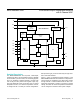
Figure 3a. Voltage Conversion Timing Diagram
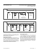
Figure 3b. Temperature Conversion Timing Diagram
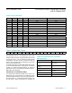
13 f
CLKs
WARMUP
3 f
CLKs
WRITE TO OUTPUT
REGISTER
INPUT
ACQUISITION
f
CLKS
SSTRB
FCLK
REF
ACQUISITION 1
REF
ACQUISITION 2
CONVERSION CYCLE 1
CONVERSION CYCLES 2–12
REFERENCE SAMPLING
13 f
CLKs
WARMUP
44 f
CLKs
CONVERSION
CYCLES 2–12
REFERENCE
SAMPLING
3 f
CLKs
SUBTRACTION
AND WRITE TO
OUTPUT REGISTER
48 f
CLKs
CONVERSION CYCLES 1–12
13 f
CLKs
WARMUP
INPUT
ACQUISITION
INPUT
ACQUISITION
SSTRB
FCLK
4 f
CLKs
CONVERSION CYCLE 1
FIRST CONVERSION
SECOND CONVERSION
MAX1098/MAX1099 10-Bit Serial-Output Temperature Sensors
with 5-Channel ADC
www.maximintegrated.com
Maxim Integrated
│
13