
Datasheet


Converter Operation
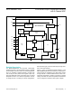
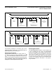
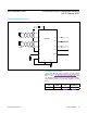
Figure 2 shows a simplified model of the converter input
structure. Once initiated, a voltage conversion requires
64 f
CLK
periods, where f
CLK
is the internal master clock.
Each conversion is preceded by 13 f
CLK
periods of warm-
up time, performed in twelve 4 f
CLK
period cycles, and
followed by three f
CLK
periods to load the output register.
SSTRB falls at the beginning of a conversion and rises at
the end of a conversion.
Inputs IN+ and IN- charge capacitors C
HOLDP
and
C
HOLDN
, respectively, during the acquisition interval that
occurs during the first f
CLK
period of the first conversion
cycle. In the second f
CLK
period, the T/H switches open
so that charge is retained on C
HOLDP
and C
HOLDN
as a
sample of the differential voltage between IN+ and IN-.
This charge is transferred to the ADC during the third and
fourth f
CLK
periods.
The reference sampling process begins in the second
conversion cycle and continues until the conversion is
complete. Sampling occurs during the second and fourth
f
CLK
periods to yield an effective doubling of the reference
voltage. The reference sampling requirement is signal
dependent and may or may not occur in every subse-
quent conversion cycle.
Temperature conversion is nothing more than subtracting
the results of two sequential voltage conversions. The
only difference is that output registers are not loaded at
the end of the first conversion. Thus, temperature conver-
sions require 2 x 64 - 3 = 125 f
CLK
periods. Figures 3a
and 3b show timing diagrams for voltage and temperature
conversions, respectively.
Track/Hold
The T/H stage for the MAX1098/MAX1099 is a simple
switched-capacitor sampling operation. The time required
for the T/H stage to acquire an input signal is a function
of how fast its input capacitance is charged. If the signal
source impedance is high, the acquisition time lengthens
and more time must be allowed between conversions.
The acquisition time (t
ACQ
) is the maximum time the
device takes to acquire the signal. Calculate this with the
following equation:
t
ACQ
= 7 (R
s
+ R
IN
) C
IN
where R
s
is the source impedance of the input signal,
R
IN
is the T/H input impedance (40kΩ), and C
IN
is the
Figure 2. Converter Input Structure
TIMING/CONTROL
LOGIC
FULLY
DIFFERENTIAL
A/D
OUTPUT
GAIN
OF 2
IN+
IN-
REF
TRACK AND HOLD
C
HOLDP
4pF
C
HOLDN
4pF
C
REF
4pF
R
R
30kΩ
R
IN
40kΩ
R
IN
40kΩ
T/H
T/H
MAX1098/MAX1099 10-Bit Serial-Output Temperature Sensors
with 5-Channel ADC
www.maximintegrated.com
Maxim Integrated
│
12