
Datasheet


Internal Clock Mode
Select internal clock mode to release the µP from the
burden of running the SAR conversion clock. To select
this mode, bit D7 of the control byte must be set to 1
and bit D6 must be set to 0. The internal clock frequen-
cy is then selected, resulting in a 3.6µs conversion time.
When using the internal clock mode, connect the CLK
pin either high or low to prevent the pin from floating.
External Clock Mode
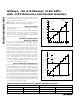
To select the external clock mode, bits D6 and D7 of the
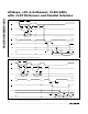
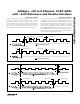
control byte must be set to one. Figure 6 shows the clock
and WR timing relationship for internal (Figure 6a) and
external (Figure 6b) acquisition modes with an external
clock. Proper operation requires a 100kHz to 7.6MHz
clock frequency with 30% to 70% duty cycle. Operating
the MAX1090/MAX1092 with clock frequencies lower
than 100kHz is not recommended, because it causes a
voltage droop across the hold capacitor in the T/H stage,
which results in degraded performance.
MAX1090/MAX1092
400ksps, +5V, 8-/4-Channel, 10-Bit ADCs
with +2.5V Reference and Parallel Interface
______________________________________________________________________________________ 13
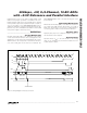
WR
CLK
CLK
WR
WR GOES HIGH WHEN CLK IS HIGH.
WR GOES HIGH WHEN CLK IS LOW.
t
CWS
t
CH
t
CL
t
CP
t
CWH
ACQUISITION STARTS
ACQUISITION STARTS
CONVERSION STARTS
CONVERSION STARTS
ACQUISITION ENDS
ACQUISITION ENDS
ACQMOD = "0"
ACQMOD = "0"
Figure 6a. External Clock and
WR
Timing (Internal Acquisition Mode)
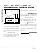
WR
CLK
CLK
WR
WR GOES HIGH WHEN CLK IS HIGH.
WR GOES HIGH WHEN CLK IS LOW.
t
DH
t
DH
t
CWH
t
CWS
ACQUISITION STARTS
ACQUISITION STARTS
CONVERSION STARTS
CONVERSION STARTS
ACQUISITION ENDS
ACQUISITION ENDS
ACQMOD = "1"
ACQMOD = "1"
ACQMOD = "0"
ACQMOD = "0"
Figure 6b. External Clock and
WR
Timing (External Acquisition Mode)