
Datasheet


MAX1084/MAX1085
400ksps/300ksps, Single-Supply, Low-Power,
Serial 10-Bit ADCs with Internal Reference
_______________________________________________________________________________________ 7
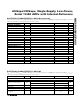
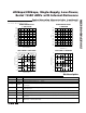
2.490
2.496
2.494
2.492
2.498
2.500
2.502
2.504
2.506
2.508
2.510
2.5 3.53.0 4.0 4.5 5.0 5.5
INTERNAL REFERENCE VOLTAGE
vs. SUPPLY VOLTAGE
MAX1084/5 toc07
SUPPLY VOLTAGE (V)
V
REF
(V)
2.490
2.496
2.494
2.492
2.500
2.498
2.508
2.506
2.504
2.502
2.510
-40-200 20406080100
INTERNAL REFERENCE VOLTAGE
vs. TEMPERATURE
MAX1084/5 toc08
TEMPERATURE (°C)
V
REF
(V)
1.50
2.00
1.75
2.50
2.25
2.75
3.00
2.5 3.5 4.03.0 4.5 5.0 5.5
SUPPLY CURRENT vs. SUPPLY VOLTAGE
MAX1084/5 toc09
SUPPLY VOLTAGE (V)
SUPPLY CURRENT (mA)
CONVERTING,
SCLK = 6.4MHz
CONVERTING,
SCLK = 4.8MHz
STATIC
CODE = 1111 1111 1111
R
L
= ∞
C
L
= 10pF
1.5
1.8
2.4
2.1
2.7
3.0
-40 0-20 20406080100
SUPPLY CURRENT vs. TEMPERATURE
MAX1084/5 toc10
TEMPERATURE (
°
C)
SUPPLY CURRENT (mA)
V
DD
= 5V, CONVERTING
V
DD
= 3V, CONVERTING
V
DD
= 5V, STATIC
V
DD
= 3V, STATIC
Typical Operating Characteristics (continued)
(MAX1084: V
DD
= +5.0V, f
SCLK
= 6.4MHz; MAX1085: V
DD
= +3.0V, f
SCLK
= 4.8MHz; C
LOAD
= 20pF, 4.7µF capacitor at REF,
T
A
= +25°C, unless otherwise noted.)
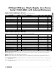
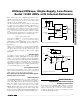
Pin Description
Serial-Clock Input. SCLK drives the conversion process and clocks data out at rates up to 6.4MHz
(MAX1084) or 4.8MHz (MAX1085).
PIN
Positive Supply VoltageV
DD
1
FUNCTIONNAME
Sampling Analog Input, 0 to V
REF
RangeAIN2
Analog and Digital GroundGND5
Active-Low Chip Select. Initiates conversions on the falling edge. When CS is high, DOUT is high
impedance.
CS
7
Reference Voltage for Analog-to-Digital Conversion. Internal 2.5V reference output. Bypass with a
4.7µF capacitor.
REF4
Active-Low Shutdown Input. Pulling SHDN low shuts down the device and reduces the supply current
to 2µA (typ).
SHDN
3
SCLK8
Serial-Data Output. DOUT changes state at SCLK’s rising edge. High impedance when CS is high.
DOUT6