
Datasheet


MAX1084/MAX1085
400ksps/300ksps, Single-Supply, Low-Power,
Serial 10-Bit ADCs with Internal Reference
12 ______________________________________________________________________________________
3) Pull
CS
high at or after the 13th rising clock edge. If
CS
remains low, the two sub-bits and trailing zeros
are clocked out after the LSB.
4) With
CS
= high, wait the minimum specified time, t
CS
,
before initiating a new conversion by pulling
CS
low.
If a conversion is aborted by pulling
CS
high before
the conversion completes, wait the minimum acquisi-
tion time, t
ACQ
, before starting a new conversion.
CS
must be held low until all data bits are clocked out.
Data can be output in 2 bytes or continuously, as shown
in Figure 8. The bytes contain the result of the conversion
padded with three leading zeros, 2 sub-bits, and trailing
zeros if SCLK is still active with CS kept low.
SPI and Microwire
When using SPI or QSPI, set CPOL = 0 and CPHA = 0.
Conversion begins with a
CS
falling edge. DOUT goes
low, indicating a conversion is in progress. Two con-
secutive 1-byte reads are required to get the full 10+2
bits from the ADC. DOUT output data transitions on
SCLK’s rising edge and is clocked into the µP on the
following rising edge.
The first byte contains 3 leading zeros, and 5 bits of
conversion result. The second byte contains the remain-
ing 5 bits, 2 sub-bits, and 1 trailing zero. See Figure 11
for connections and Figure 12 for timing.
QSPI
Unlike SPI, which requires two 1-byte reads to acquire
the 10 bits of data from the ADC, QSPI allows the mini-
mum number of clock cycles necessary to clock in the
data. The MAX1084/MAX1085 require 13 clock cycles
from the µP to clock out the 10 bits of data. Additional
clock cycles clock out the 2 sub-bits followed by trailing
zeros. Figure 13 shows a transfer using CPOL = 0 and
CPHA = 1. The result of conversion contains two zeros
followed by the 10 bits of data in MSB-first format.
Layout and Grounding
For best performance, use PC boards. Wire-wrap
boards are not recommended. Board layout should
ensure that digital and analog signal lines are separat-
ed from each other. Do not run analog and digital
(especially clock) lines parallel to one another, or digital
lines underneath the ADC package.
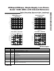
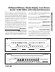
11…111
11…110
11…101
00…011
00…010
00…001
00…000
012 FS
OUTPUT CODE
FS - 3/2LSBINPUT VOLTAGE (LSB)
1LSB =
V
REF
1024
FS = V
REF
FULL-SCALE
TRANSITION
3
Figure 10. Unipolar Transfer Function, Full Scale (FS) = V
REF
,
Zero Scale (ZS) = GND
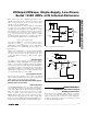
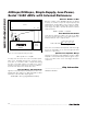
CS
SCLK
DOUT
I/O
SCK
MISO
+3V OR +5V
SS
a) SPI
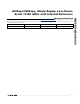
CS
SCLK
DOUT
CS
SCK
MISO
+3V OR +5V
SS
b) QSPI
MAX1084
MAX1085
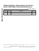
MAX1084
MAX1085
MAX1084
MAX1085
CS
SCLK
DOUT
I/O
SK
SI
c) MICROWIRE
Figure 11. Common Serial-Interface Connections to the
MAX1084/MAX1085