
Datasheet

MAX1032/MAX1033
8- and 4-Channel, ±3 x V
REF
Multirange Inputs, Serial 14-Bit ADCs
6
Maxim Integrated
Note 1: Parameter tested at V
AVDD1
= V
AVDD2
= V
DVDD
= V
DVDD0
= 5V.
Note 2: See definitions in the
Parameter Definitions
section at the end of the data sheet.
Note 3: Guaranteed by correlation with single-ended measurements.
Note 4: Not production tested. Guaranteed by design.
Note 5: To ensure external reference operation, V
REFCAP
must exceed (V
AVDD1
- 0.1V). To ensure internal reference operation, V
REFCAP
must be below (V
AVDD1
- 0.4V). Bypassing REFCAP with a 0.1μF or larger capacitor to AGND1 sets V
REFCAP
≈ 4.096V. The tran-
sition point between internal reference mode and external reference mode lies between the REFCAP buffer disable threshold
minimum and maximum values (Figures 17 and 18).
Note 6: The SCLK duty cycle can vary between 40% and 60%, as long as the t
CL
and t
CH
timing requirements are met.
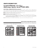
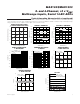
ANALOG SUPPLY CURRENT
vs. ANALOG SUPPLY VOLTAGE
MAX1032 toc01
V
AVDD1
(V)
I
AVDD1
(mA)
5.155.054.954.85
2.2
2.3
2.4
2.5
2.6
2.1
4.75 5.25
EXTERNAL CLOCK MODE
T
A
= +85°C
T
A
= +25°C
T
A
= -40°C
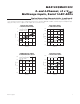
PREAMPLIFIER SUPPLY CURRENT
vs. PREAMPLIFIER SUPPLY VOLTAGE
MAX1032 toc02
V
AVDD2
(V)
I
AVDD2
(mA)
5.155.054.85 4.95
11
12
13
14
16
15
17
18
10
4.75 5.25
EXTERNAL CLOCK MODE
AIN1–AIN7 = AGND2
AIN0 = +FS
T
A
= +85°C
T
A
= +25°C
T
A
= -40°C
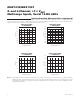
DIGITAL I/O SUPPLY CURRENT
vs. DIGITAL I/O SUPPLY VOLTAGE
MAX1032 toc04
V
DVDDO
(V)
I
DVDDO
(µA)
5.155.054.954.85
17
18
19
20
21
16
4.75 5.25
T
A
= +85°C
T
A
= +25°C
T
A
= -40°C
EXTERNAL CLOCK MODE
DATA RATE = 115ksps
Typical Operating Characteristics
(V
AVDD1
= V
AVDD2
= V
DVDD
= V
DVDD0
= 5V, V
AGND1
= V
DGND
= V
DGNDO
= V
AGND2
= V
AGND3
= 0V, f
CLK
= 3.5MHz (50% duty
cycle), external clock mode, V
REF
= 4.096V (external reference operation), REFCAP = AVDD1, maximum single-ended bipolar input
range (±3 x V
REF
), C
DOUT
= 50pF, C
SSTRB
= 50pF; unless otherwise noted.)
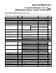
ELECTRICAL CHARACTERISTICS (continued)
(V
AVDD1
= V
AVDD2
= V
DVDD
= V
DVDD0
= 5V, V
AGND1
= V
DGND
= V
DGNDO
= V
AGND2
= V
AGND3
= 0V, f
CLK
= 3.5MHz (50% duty
cycle), external clock mode, V
REF
= 4.096V (external reference operation), REFCAP = AVDD1, maximum single-ended bipolar input
range (±3 x V
REF
), C
DOUT
= 50pF, C
SSTRB
= 50pF, T
A
= -40°C to +85°C, unless otherwise noted. Typical values are at T
A
= +25°C.)