
Datasheet


MAX1032/MAX1033
8- and 4-Channel, ±3 x V
REF
Multirange Inputs, Serial 14-Bit ADCs
13
Maxim Integrated
Detailed Description
The MAX1032/MAX1033 multirange, low-power, 14-bit
successive-approximation ADCs operate from a single
+5V supply and have a separate digital supply allowing
digital interface with 2.7V to 5.25V systems. These 14-bit
ADCs have internal track-and-hold (T/H) circuitry that
supports single-ended and fully differential inputs. For
single-ended conversions, the valid analog input voltage
range spans from -3 x V
REF
below ground to +3 x V
REF
above ground. The maximum allowable differential input
voltage spans from -6 x V
REF
to +6 x V
REF
. Data can be
converted in a variety of software-programmable chan-
nel and data-acquisition configurations. Microprocessor
(μP) control is made easy through an SPI-/QSPI-/
MICROWIRE-compatible serial interface.
The MAX1032 has eight single-ended analog input
channels or four differential channels (see the
Block
Diagram
at the end of the data sheet). The MAX1033 has
four single-ended analog input channels or two differential
channels. Each analog input channel is independently soft-
ware programmable for seven single-ended input ranges
(0 to (3 x V
REF
)/2, (-3 x V
REF
)/2 to 0, 0 to 3 x V
REF
, -3 x
V
REF
to 0, (±3 x V
REF
)/4, (±3 x V
REF
)/2
,
±3 x V
REF
) and
three differential input ranges (±3 x V
REF
)/2, ±3 x V
REF,
±6
x V
REF
. Additionally, all analog input channels are fault tol-
erant to ±16.5V. A fault condition on an idle channel does
not affect the conversion result of other channels.
Pin Description (continued)
PIN
MAX1032 MAX1033
NAME FUNCTION
22 19 AVDD2
Analog Supply Voltage 2. Connect AVDD2 to a 4.75V to 5.25V power-supply voltage. Bypass
AVDD2 to AGND2 with a 0.1μF capacitor.
23 20 AGND2
Analog Ground 2. This ground carries approximately five times more current than AGND1.
DGND, DGNDO, AGND3, AGND2, and AGND1 must be connected together.
24 1 AGND1 Anal og Gr ound 1. D GN D , D GN DO, AGN D 3, AGN D 2, and AGND 1 must b e connected together .
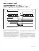
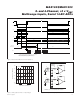
4–20mA
PLC
ACCELERATION
PRESSURE
TEMPERATURE
WHEATESTONE
WHEATESTONE
1μF
0.1μF
AGND2
DGNDOAGND3 DGND
AVDD2
DVDD
AVDD1
0.1μF 0.1μF 0.1μF
5.0V 5.0V 5.0V
MAX1032
CHO
CH1
CH2
CH3
CH4
CH5
CH6
CH7
REF
AGND1
REFCAP
0.1μF
3.3V
MC68HCXX
μC
DVDD0
SCLK
CS
DIN
SSTRB
DOUT
V
DD
SCK
I/O
MOSI
I/O
MISO
V
SS
Figure 1. Typical Application Circuit