
Users Guide: Network Microcontroller Supplement User Manual

High-Speed Microcontroller User’s
Guide: Network Microcontroller
Supplement
92
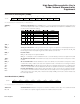
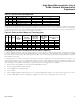
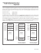
7 6543210
SFR F9h P7.7 P7.6 P7.5 P7.4 P7.3 P7.2 P7.1 P7.0
RW-1 RW-1 RW-1 RW-1 RW-1 RW-1 RW-1 RW-1
7 6543210
SFR FBh TL3.7 TL3.6 TL3.5 TL3.4 TL3.3 TL3.2 TL3.1 TL3.0
RW-0 RW-0 RW-0 RW-0 RW-0 RW-0 RW-0 RW-0
76543210
SFR FCh TH3.7 TH3.6 TH3.5 TH3.4 TH3.3 TH3.2 TH3.1 TH3.0
RW-0 RW-0 RW-0 RW-0 RW-0 RW-0 RW-0 RW-0
Parallel I/O Port 7 (P7)
R = Unrestricted read, W = Unrestricted write, -n = Value after reset (P7._ above)
Timer 3 LSB (TL3)
R = Unrestricted read, W = Unrestricted write, -n = Value after reset
Timer 3 MSB (TH3)
R = Unrestricted read, W = Unrestricted write, -n = Value after reset
P7.7–0
Bits 7–0
Port 7 bits 7–0. This port is a programmable parallel I/O port. Data written to the port latch serves to set
both logic level and direction of the data on the pin. A 1 written to a port latch, previously programmed
to a 0, activates a high-current, one-shot pullup on the corresponding pin. This is followed by a static,
low-current pullup, which remains on until the port is changed again. The final high state of the port pin
is considered a pseudo-input mode and can be easily overdriven from an external source. Port latches
previously in a high-output state do not change, nor does the high-current one-shot fire when a 1 is
loaded. Loading a 0 to a port latch results in a static, high-current pulldown on the corresponding pin.
This mode is termed the I/O output state, since no weak devices are used to drive the pin. Port 7 func-
tions as the nonmultiplexed external address output port for addresses A0–A7 when MUX = 1.
TL3.7–0
Bits 7–0
Timer 3 LSB. This register is used to load and read the least significant 8-bit value in timer 3.
TH3.7–0
Bits 7–0
Timer 3 MSB. This register is used to load and read the most significant 8-bit value in timer 3.
Maxim Integrated