
Users Guide: Network Microcontroller Supplement User Manual

High-Speed Microcontroller User’s
Guide: Network Microcontroller
Supplement
88
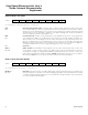
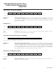
76543210
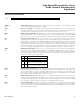
SFR EDh DPX3.7 DPX3.6 DPX3.5 DPX3.4 DPX3.3 DPX3.2 DPX3.1 DPX3.0
RW-0 RW-0 RW-0 RW-0 RW-0 RW-0 RW-0 RW-0
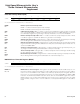
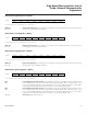
7 6543210
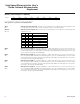
SFR EBh DPX2.7 DPX2.6 DPX2.5 DPX2.4 DPX2.3 DPX2.2 DPX2.1 DPX2.0
RW-0 RW-0 RW-0 RW-0 RW-0 RW-0 RW-0 RW-0
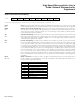
76543210
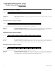
SFR EEh — — — — —
OWMAD.2
OWMAD.1
OWMAD.0
RW-0 RW-0 RW-0 RW-0 RW-0 RW-1 RW-1 RW-1
Data Pointer Extended Register 2 (DPX2)
R = Unrestricted read, W = Unrestricted write, -n = Value after reset
Data Pointer Extended Register 3 (DPX3)
R = Unrestricted read, W = Unrestricted write, -n = Value after reset
1-Wire Master Address Register (OWMAD)
R = Unrestricted read, W = Unrestricted write, -n = Value after reset
DPX2.7–0
Bits 7–0
Data pointer extended byte 2. This register contains the high-order byte of the extended 24-bit address
for auxiliary data pointer 2. This register is used only in the 24-bit paged and contiguous addressing
modes. This register is not used for addressing the data memory in the 16-bit addressing mode and,
therefore, can be utilized as a scratchpad SRAM register.
DPX3.7–0
Bits 7–0
Data pointer extended byte 3. This register contains the high-order byte of the extended 24-bit address
for auxiliary data pointer 3. This register is used only in the 24-bit paged and contiguous addressing
modes. This register is not used for addressing the data memory in the 16-bit addressing mode and,
therefore, can be utilized as a scratchpad SRAM register.
Bits 7–3
OWMAD.2-0
Bits 2-0
Reserved. (Read returns all zeros.)
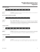
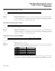
1-Wire master address select bits 2-0. These bits are used to select one of the five 1-Wire master reg-
isters to be accessed by the OWMDR SFR. Prior to accessing any of the 1-Wire master’s registers, the
address of the target register must be specified as following:
The 1-Wire master supports only the above address values. When these bits are set to states other than
those listed above, read data in the OWMDR is invalid, and write data to the OWMDR does not change
the logic state of any of the five registers. Note that the default values for these bits are set to 111b.
A2
A1
A0
REGISTER ACCESS MODE
0
0
0
Command register Read/write
0
0
1
Receive/transmit buffer
Read (receive)/write (transmit)
0
1
0
Interrupt flag register Read
0
1
1
Interrupt enable register
Read/write
1
0
0
Clock divisor register Read/write
1
0
1
Control register Read/write
Maxim Integrated