
Users Guide: Network Microcontroller Supplement User Manual

High-Speed Microcontroller User’s
Guide: Network Microcontroller
Supplement
71
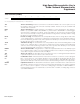
Bit 4
PDCE3
Bit 3
PDCE2
Bit 2
PDCE1
Bit 1
PDCE0
Bit 0
Reserved.
Program/data chip enable 3. PDCE3 provides the software selection for CE3 to be used with either pro-
gram or program and data memory when CE3 is enabled by the port 4 control register (P4CNT). PDCE3
becomes a “don’t care” when CE3 is not enabled. The port 4 contr
ol register SFR establishes the spe-
cific address range for CE3. Write access to the memory block, which is connected to CE3 as data
memory (PDCE3 = 1), comes fr
om the P3.6 WR signal. A read of the memory block connected to CE3
as program and data memory (PDCE3 = 1) comes from the PSEN signal, as opposed to the normal P3.7
RD signal when doing data memory r
eads.
PDCE3 = 0 enables CE3 as a program memory chip enable.
PDCE3 = 1 enables CE3 as a merged program and data memory chip enable.
Program/data chip enable 2. PDCE2 provides the software selection for CE2 to be used with either pro-
gram or program and data memory when CE2 is enabled by the port 4 contr
ol register (P4CNT). PDCE2
becomes a “don’t care” when CE2 is not enabled. The port 4 control register SFR establishes the spe-
cific address range for CE2
. Write access to the memory block, which is connected to CE2 as data
memory (PDCE2 = 1), comes from the P3.6 WR signal. A read of the memory block connected to CE2
as pr
ogram and data memory (PDCE2 = 1) comes from the PSEN signal, as opposed to the normal P3.7
RD signal when doing data memory r
eads.
PDCE2 = 0 enables CE2 as a program memory chip enable.
PDCE2 = 1 enables CE2 as a merged program and data memory chip enable.
Program/data chip enable 1. PDCE1 provides the software selection for CE1 to be used with either pro-
gram or program and data memory when CE1 is enabled by the port 4 control register (P4CNT). PDCE1
becomes a “don’t care” when
CE1 is not enabled. The port 4 control register SFR establishes the spe-
cific address range for CE1. Write access to the memory block, which is connected to CE1 as data
memory (PDCE1 = 1), comes fr
om the P3.6 WR signal. A read of the memory block connected to CE1
as program and data memory (PDCE1 = 1) comes from the PSEN signal, as opposed to the normal P3.7
RD signal when doing data memory reads.
PDCE1 = 0 enables CE1 as a program memor
y chip enable.
PDCE1 = 1 enables CE1 as a merged program and data memory chip enable.
Program/data chip enable 0. PDCE0 pr
ovides the software selection for CE0 to be used with either pro-
gram or program and data memory when CE0 is enabled by the por
t 4 control register (P4CNT). PDCE0
becomes a “don’t care” when CE0 is not enabled. The port 4 control register SFR establishes the spe-
cific address range for CE0. Write access to the memor
y block, which is connected to CE0 as data
memory (PDCE0 = 1), comes from the P3.6 WR signal. A read of the memory block connected to CE0
as pr
ogram and data memory (PDCE0 = 1) comes from the PSEN signal, as opposed to the normal P3.7
RD signal when doing data memory reads.
PDCE0 = 0 enables CE0 as a program memory chip enable.
PDCE0 = 1 enables CE0 as a merged program and data memor
y chip enable.
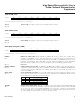
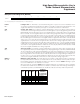
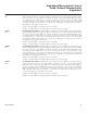
Timed-Access Register (TA)
W = Unrestricted write, -n = Value after reset
76543210
SFR C7h TA.7 TA.6 TA.5 TA.4 TA.3 TA.2 TA.1 TA.0
RW-1 RW-1 RW-1 RW-1 RW-1 RW-1 RW-1 RW-1
TA.7–0
Bits 7–0
This register provides a timed-control sequence for software writes to some special register bits, in order
to protect against inadvertent changes to configuration and to the program memory in the event of a
loss of software control.
Maxim Integrated