
Users Guide: Network Microcontroller Supplement User Manual

High-Speed Microcontroller User’s
Guide: Network Microcontroller
Supplement
44
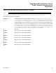
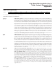
Port 5 Control Register (P5CNT)
76543210
SFR A2h — CAN0BA — — C0_I/O P5CNT.2 P5CNT.1 P5CNT.0
RW-1 RW-0 RW-0 RW-0 RW-0 RT-0 RT-0 RT-0
R = Unrestricted read, W = Unrestricted write, T = Timed Access Write Only, -n = Value after reset
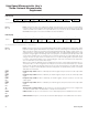
Bit 7
CAN0BA
Bit 6
Bit 5
Bit 4
C0_I/O
Bit 3
P5CNT.2-P5CNT.0
Bits 2-0
Reserved. Read returns logic 1.
CAN 0 bus active status. The CAN0BA signal is a latched status bit that is set if the respective CAN 0
I/O-enabled (P5CNT.3) bit is set and bus activity is detected on the CAN 0 bus. Once activity is detect-
ed and the bit is set, it remains set until cleared by application software or a reset. This bit is not used
on the DS80C411 and returns an indeterminate value.
Reserved. Read returns logic 0.
Reserved. Read returns logic 0.
CAN 0 I/O enable. The P5CNT.3 bit configur
es P5.0 and P5.1 as either standar
d I/O or CAN receive input
(P5.1–C0RX) and CAN transmit output (P5.0–C0TX). Programming P5CNT.3 to a 0 places P5.1 and P5.0 into
the standard I/O mode. Programming P5CNT.3 to a 1 places P5.1 and P5.0 into the CAN transmit and receive
mode. When P5CNT.3 is programmed to a 1, all I/O interaction through the port 5 SFR with P5.1 and P5.0 is
disabled. This bit must be set to 1 on the DS80C411.
Port pin P5.7–P5.4 configuration control bits. Once any bit combination containing a 1 is pr
o-
grammed into P5CNT.2-P5CNT.0, the corresponding port pins that are then assigned to peripheral chip
enable are locked out from being programmed as I/O in the port 5 SFR. The internally decoded range
for each peripheral chip enable (PCE0–PCE3) is established by the number of external addr
ess lines
(A19–A16), which are enabled by the P6CNT.5-P6CNT.3 control bits. This can be different than the pro-
gram memory CE0–CE7 decoding. The following table outlines the assigned data memory boundaries
of each chip enable as determined by the P6CNT.5-P6CNT.3 control bits. Note that, when the external
address bus is limited to A0–A15, the chip enables are internally decoded on a 32kB x 8 block bound-
ar
y. This is to allow the use of the more common memories, as opposed to using a less common 64kB
block size memory.
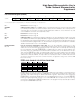
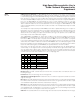
PCEx CHIP-ENABLE SELECTION FUNCTION
PCE0–PCE3 are internally decoded to data memory address block boundaries as determined by the
P6CNT.5–P6CNT.3 control bits. When any of CE0–CE7 are converted from a program chip enable to pro-
gram/data chip enables through the MCON and MCON1 registers, data memory areas assigned to
PCE0–PCE3 are automatically disabled when the corresponding memory area is covered by CE0–CE7.
Enabling merged program/data memory access under CE0–CE7 does not alter the port 5 control reg-
ister bit states. Returning the CE0–CE7 enables back to the program memory automatically reenables
the respective PCE0–PCE3 relationship.
P5CNT.2-0
P5.7 P5.6 P5.5 P5.4
000 I/O I/O I/O I/O
100 I/O I/O I/O PCE0
101 I/O I/O PCE1 PCE0
110 I/O PCE2 PCE1 PCE0
111 PCE3 PCE2 PCE1 PCE0
Maxim Integrated