
Users Guide: Network Microcontroller Supplement User Manual

High-Speed Microcontroller User’s
Guide: Network Microcontroller
Supplement
35
Data Pointer Extended Register 0 (DPX)
Data Pointer Extended Register 1 (DPX1)
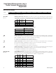
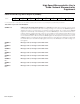
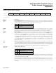
Program Memory Chip-Enable Boundaries
P4CNT.5-3
CE0 CE1 CE2 CE3 CE4 CE5 CE6 CE7
000 32K 32-64K 64-96K 96-128K 128-160K 160-192K 192-224K 224-256K
001 128K 128-256K 256-384K 384-512K 512-640K 640-768K 768-896K
896-1024K
010 256K 256-512K 512-768K
768-1024K
1024-1280K
1280-1536K
1536-1792K
1792-2048K
011 512K .512-1M 1-1.5M 1.5-2M 2-2.5M 2.5-3M 3-3.5M 3.5-4M
100 1M 1-2M 2-3M 3-4M 4-5M 5-6M 6-7M 7-8M
101 2M 2-4M 4-6M 6-8M 8-10M 10-12M 12-14M 14-16M
110 or 111
4M 4-8M 8-12M 12-16M — — — —
P4CNT.2-P4CNT.0 Port pin P4.3–P4.0 configuration control bits. P4CNT.2-0 determines whether specific P4 pins
function as program chip-enable signals or I/O. The memory ranges for each CEx signal are determined
by P4CNT.5-3. Note that, when the appropriate PDCEx bit (MCON.3–0) is set, the corresponding CEx
pin functions as a combined program/peripheral chip enable, and the respective PCE0–PCE3 is dis-
abled. CE4–CE7 are enabled via P6CNT.2–0.
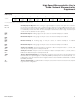
CE0–CE3 Chip-Enable Function Selection
P4CNT.2-0
P4.3 P4.2 P4.1 P4.0
000 I/O I/O I/O I/O
100 I/O I/O I/O CE0
101 I/O I/O CE1 CE0
110 I/O CE2 CE1 CE0
111 CE3 CE2 CE1 CE0
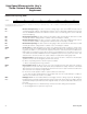
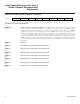
76543210
SFR 93h DPX.7 DPX.6 DPX.5 DPX.4 DPX.3 DPX.2 DPX.1 DPX.0
RW-0 RW-0 RW-0 RW-0 RW-0 RW-0 RW-0 RW-0
R = Unrestricted read, W = Unrestricted write, -n = Value after reset
DPX.7–0
Bits 7–0
Data pointer extended register 0. This register contains the high-order byte of the extended 24-bit
address for data pointer 0. This register is used only in the 24-bit paged and contiguous addressing
modes. This register is not used for addressing the data memory in the 16-bit addressing mode and,
therefore, can be utilized as a scratchpad SRAM register.
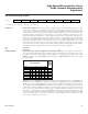
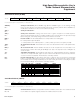
DPX1.7–0
Bits 7–0
Data pointer extended register 1. This register contains the high-order byte of the extended 24-bit
address for auxiliary data pointer 1. This register is used only in the 24-bit paged and contiguous
addressing modes. This register is not used for addressing the data memory in the 16-bit addressing
mode and, therefore, can be utilized as a scratchpad SRAM register.
76543210
SFR 95h DPX1.7 DPX1.6 DPX1.5 DPX1.4 DPX1.3 DPX1.2 DPX1.1 DPX1.0
RW-0 RW-0 RW-0 RW-0 RW-0 RW-0 RW-0 RW-0
R = Unrestricted read, W = Unrestricted write, -n = Value after reset
Maxim Integrated