
Users Guide: Network Microcontroller Supplement User Manual

High-Speed Microcontroller User’s
Guide: Network Microcontroller
Supplement
124
ADDENDUM TO SECTION 12: SERIAL I/O
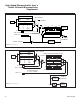
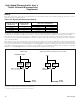
The DS80C400 high-speed microcontroller provides a third fully independent UART (serial port 2) nearly identical to the second serial
port (serial port 1). The transmit and receive pins associated with the third serial port are alternate functions for P6.7 (TXD2) and P6.6
(RXD2). The primary functional difference between the third serial port and the previous two is that it can only use timer 3 for baud clock
generation in asynchronous serial modes 1 and 3.
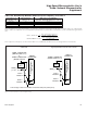
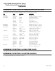
The third UART has its own control register (SCON2: FEh) and transmit/receive buffer (SBUF2: FFh). These two registers, and others
related to operation of the third serial port, are summarized in Table 12-1.
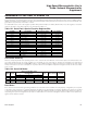
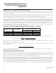
Table 12-1. Serial Port 2 Special Function Registers/Bits
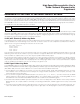
Serial Mode Summary
All three serial ports provide four operating modes. These serial modes offer different communication protocols and baud rates. The
four serial operating modes are shown in Table 12-2. Full details of each serial mode of operation are provided in the High-Speed
Microcontroller User’s Guide. The DS80C400 includes a clock multiplier that, when utilized, can affect the serial baud clock for certain
modes. Provisions for use of the serial ports in conjunction with the clock multiplier and power-management mode are discussed later
in this section.
Table 12-2. Serial I/O Modes
†
Use of the clock multiplier or power-management mode affects the baud clock.
Baud Rates
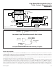
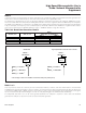
Each serial mode has baud-rate-generating hardware associated with it. This hardware must be properly configured by the user prior
to operation of the serial port. The following baud-rate descriptions are separated by mode. Block diagrams have also been included
to show any deviations from the diagrams included in the High-Speed Microcontroller User’s Guide. Note that the baud clock input cor-
responding to the power-management mode has been omitted from each of the block diagrams. Reference Table 12-3 for power-man-
agement mode baud clock rates.
BAUD CLOCK OPTIONS LISTED
BY SERIAL PORT
†
SERIAL
MODE
SYNC/
ASYNC
012
DATA
BITS
START/STOP BITS
9TH BIT
FUNCTION
0 Sync 4t
CLK
or 12t
CLK
8 None None
1
Async
Timer 1 or 2 Timer 1 Timer 3 8 1 start, 1 stop None
2
Async
32t
CLK
or 64t
CLK
9 1 start, 1 stop 0, 1, parity
3
Async
Timer 1 or 2 Timer 1 Timer 3 9 1 start, 1 stop 0, 1, parity
BIT NAM ES D E SCRI PTION REGISTER LOCATION BIT PO SITIONS
SM0/FE _2
Serial mod e s el e c t 0 or fram i ng
SCON2–FEh SCON2.7
SM1_ 2 Seria l m ode selec t 1 SCON2– FEh SCON2.6
SM2_ 2 Seria l m ode selec t 2 SCON2– FEh SCON2.5
REN_ 2 R e c e ive e n ab le SCON2 – FEh SCON2.4
TB 8_ 2 9th trans mi t data b it SCON2–FEh SCON2.3
R B 8_ 2 9t h receive dat a b it SCON2–FEh SCON2.2
TI _ 2 Tran s mi t in t errupt flag SCON2– FEh SCON2.1
R1_ 2 R e c e iv e i n t errupt flag SCON2–FEh SCON2.0
SMOD _2 B a ud-rate doubl er bit T3CM–FDh T3CM. 4
SPTA2 Serial port 2 trans mi t act ivity STATUS 1 –F 7 h STA TUS1.1
SPRA2 Seri a l p ort 2 receive ac t i vi ty STATUS1 – F 7 h STA TUS1.0
SMOD0 Fram ing error-detectio n e n ab le PCON–87 h PCON.6
— S erial dat a buff er SBUF2– F F h —
— S la v e address m a sk e n able SADEN2– F1 h —
— S la v e address SADD R2 – D 9h —
Maxim Integrated