
Users Guide: Network Microcontroller Supplement User Manual

High-Speed Microcontroller User’s
Guide: Network Microcontroller
Supplement
104
DS80C400
P7.3/A3
P7.4/A4
P7.5/A5
P7.6/A6
P7.7/A7
Vcc1
EA\
ALE
PSEN\
P2.0\A8
P2.1\A9
P2.2\A10
Vss
Vcc3
P2.3/A11
P2.4/A12
P2.5/A13
P2.6/A14
P2.7/A15
P6.0/CE4
P6.1/CE5
P6.2/CE6
P6.3/CE7
P6.4/A20
P6.5/A21
CRS
COL
TXD.3
TXD.2
TXD.1
TXD.0
TX_EN
TXCLK
RX_ER
RXCLK
RX_DV
Vcc3
Vss
RXD.0
RXD.1
RXD.2
RXD.3
MDC
MDIO
P3.0/RXD0
P3.1/TXD0
P3.2/INT0
P3.3/INT1
P3.4/T0
P3.5/T1/CLKO
OWSTP\
OW
RSTOL
RST
P1.7/INT5
P1.6/INT4
P1.5/INT3
P1.4/INT2
P1.3/TXD1
P1.2/RXD1
P1.1/T2EX
P1.0/T2
Vss
Vcc3
P0.0/D0
P0.1/D1
P0.2/D2
P0.3/D3
P0.4/D4
P0.5/D5
P0.6/D6
P0.7/D7
P7.0/A0
P7.1/A1
P7.2/A2
P3.6/WR
P3.7/RD
P5.7/PCE3
P5.6/PCE2
P5.5/PCE1
P5.4/PCE0
P5.3
P5.2/T3
P5.1/C0RX
P5.0/C0TX
Vcc3
XTAL2
XTAL1
Vss
MUX\
P4.7/A19
P4.6/A18
P4.5/A17
P4.4/A16
P4.3/CE3
P4.2/CE2
P4.1/CE1
P4.0/CE0
P6.7/TXD2
P6.6/RXD2
D0–D7
256kB x 8
Flash program
memory
(configurable
as data
memory)
A0–A7
A8–A15
A16
A17
OE\
CE\
WE\
D0–D7
256kB x 8
Flash program
memory
(configurable
as data
memory)
A0–A7
A8–A15
A16
A17
OE\
CE\
WE\
D0–D7
256kB x 8
Dedicated
data memory
or peripheral
memory
A0–A7
A8–A15
A16
A17
OE\
CE\
WE\
Vcc3
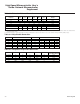
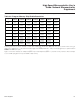
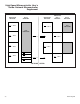
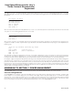
Figure 6-5. Demultiplexed Address/Data Bus
Using The Combined Chip-Enable Signals
The DS80C400 incorporates a feature allowing PCEx and CEx signals to be combined to provide a merged external program/data
memory area. Setting the one or more PDCE7–PDCE0 bits (MCON1.3–0 and MCON.3–0) causes the corresponding chip-enable sig-
nal to be asserted for both MOVC and MOVX operations. Write access to combined program and data memory blocks is controlled
by the WR signal, and read access is controlled by the PSEN signal. This feature is especially useful if the design achieves in-system
reprogrammability through external flash memory, where a single device can be accessed through both MOVC instructions (program
fetch) and MOVX write operations (updates to code memory). Figures 6-6 through 6-10 illustrate some examples of merged pro-
gram/data memor
y configurations.
Maxim Integrated