
Users Guide: Network Microcontroller Supplement User Manual

High-Speed Microcontroller User’s
Guide: Network Microcontroller
Supplement
101
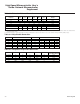
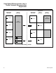
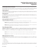
Table 6-3. Extended Address Generation
1
Only 32kB of memory is accessible per chip enable for the P4CNT.5-3 = 000b setting, which means at least two chip enables are needed to address the standard 16-bit
(0–FFFFh) address range.
2
The default P4CNT.5-3 = 111b setting (4MB accessible per CE) requires only four chip enables to access the maximum 24-bit (0–FFFFFFh) address range.
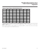
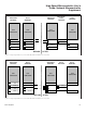
Table 6-4. Chip-Enable Generation
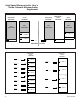
Table 6-5. Peripheral Chip-Enable Generation
P5CNT.2-0 P5.7 P5.6 P5.5 P5.4 P6CNT.5-3
MAX MEMORY
ACCESSIBLE PER PCE
000 (default)
I/O I/O I/O I/O 000 32kB
100 I/O I/O I/O PCE0 001 128kB
101 I/O I/O PCE1 PCE0 010 256kB
110 I/O PCE2 PCE1 PCE0 011 512kB
111 PCE3 PCE2 PCE1 PCE0 100 1MB
PORT PIN 6 FUNCTION PORT PIN 4 FUNCTION
P6CNT.2-0 P6.3 P6.2 P6.1 P6.0 P4CNT.2-0 P4.3 P4.2 P4.1 P4.0
000 (default) I/O I/O I/O I/O 000 I/O I/O I/O I/O
100 I/O I/O I/O CE4 100 I/O I/O I/O CE0
101 I/O I/O CE5 CE4 101 I/O I/O CE1 CE0
110 I/O CE6 CE5 CE4 110 I/O CE2 CE1 CE0
111 CE7 CE6 CE5 CE4 111 (default) CE3 CE2 CE1 CE0
P4CNT.5-3 P6.5 P6.4 P4.7 P4.6 P4.5 P4.4
MAX MEMORY ACCESSIBLE
PER CE
000 I/O I/O I/O I/O I/O I/O 32kB
1
001 I/O I/O I/O I/O I/O A16 128kB
010 I/O I/O I/O I/O A17 A16 256kB
011 I/O I/O I/O A18 A17 A16 512kB
100 I/O I/O A19 A18 A17 A16 1MB
101 I/O A20 A19 A18 A17 A16 2MB
110 or 111 (default) A21 A20 A19 A18 A17 A16 4MB
2
Maxim Integrated