
Users Guide: DS80C390 Supplement Manual

High-Speed Microcontroller User’s Guide: DS80C390 Supplement
95 of 158
IMPLEMENTING A BOOTLOADER USING INTERNAL SRAM
The internal 4 KB SRAM of the DS80C390 can be used to implement a bootloader function, allowing in-
system reprogrammability. One of the difficulties of implementing a bootloader function with a Flash
memory device is that the Flash programming algorithm will not allow instruction fetches (reads) from a
device while it is being reprogrammed. The DS80C390 avoids this problem by placing the internal
SRAM in the program/data configuration and loading it with a small bootstrap loader transferred from the
external Flash memory. The bootloader software then runs out of internal SRAM while the external
memory is being reprogrammed.
The following example demonstrates the implementation with a Flash memory. The internal SRAM is
first configured as program/data memory, and a small bootloader routine is copied from the external Flash
memory into the internal SRAM. The software then jumps to the internal SRAM and begins executing the
bootloader program out of the internal SRAM. The bootloader software activates the combined
program/chip enable function, if desired, as described above to allow simplified access to the Flash
memory. The bootloader program then begins accepting bytes by the serial port or other external interface
and copies them by MOVX instructions to the appropriate location in the external Flash until the new
program is loaded. The final step is to jump to the starting location in the external Flash and begin
execution of the new program. Soon after starting the new program software should disable the combined
program/chip enable function and configure the 4 KB SRAM as desired.
The bootloading process is summarized below. Steps 1-4 are performed while executing code from the
Flash device.
1. Set/clear CMA bit as desired.
2. Configure 4 KB SRAM as program/data. (IDM1:IDM0=11 ).
3. Copy user-supplied bootloader into 4KB SRAM.
4. LJMP to beginning of bootloader code.
5. In bootloader code, set PDCEx bits (MCON.3-0) to correspond to CEs controlling the Flash.
6. Bootloader code performs multiple MOVX operations to load new code into Flash.
7. When Flash load is complete, LJMP to starting location of new code. (This often 000000h but does
not have to be.) At beginning of new code clear PDCEx bits and configure CMA, IDM1, IDM0 as
desired.
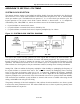
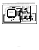
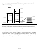
EXAMPLE DS80C390 MEMORY CONFIGURATION
The following is an example memory configuration for the DS80C390 microcontroller. Suppose that we
wish to allow 1MB of external code space by connecting a 512k x 8 memory device to each of the chip-
enable signals
CE0 , 1CE . We also want to have 1.5MB of external data memory and we achieve this by
connecting three 512k x 8 memories, one to each of the peripheral chip-enable signals
PCE0 , PCE1, and
PCE2 . Figures 6-1 and 6-2 are a rough system diagram and the corresponding program/data memory map.
Note that the memory map shows internal SRAM still located at its default address. The logical address
reanges for these internal RAMs are controlled by SFR bit settings. Users of the Keil Software PK51
compiler should consult
Application Note 606, “Configuring Keil PK51 tools to Support 24-Bit
Contiguous Addressing Mode,” for information about how to configure the compiler and
START390.A51 file.