
Users Guide: DS80C390 Supplement Manual


High-Speed Microcontroller User’s Guide: DS80C390 Supplement
9 of 158
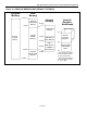
SPECIAL FUNCTION REGISTERS
Most of the unique features of the high-speed microcontroller family are controlled by bits in special
function registers (SFRs) located in unused locations in the 8051 SFR map. This allows for increased
functionality while maintaining complete instruction set compatibility. The SFRs reside in register
locations 80h-FFh and are accessed using direct addressing. SFRs that end in 0 or 8 are bit addressable.
The first table indicates the names and locations of the SFRs used by the DS80C390 and individual bits in
those registers. Bits protected by the timed-access function are shaded. The second table indicates the
reset state of all SFR bits. Following these tables is a complete description of DS80C390 SFRs that are
new to the 8051 architecture or have new or modified functionality.
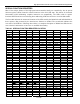
Table 4-1. SPECIAL FUNCTION REGISTER LOCATION
REGISTER BIT 7 BIT 6 BIT 5 BIT 4 BIT 3 BIT 2 BIT 1 BIT 0 ADDRESS
P4 A19/P4.7 A18/P4.6 A17/P4.5 A16/P4.4
CE3 /P4.3 CE2 /P4.2 CE1 /P4.1 CE0 /P4.0
80h
SP 81h
DPL 82h
DPH 83h
DPL1 84h
DPH1 85h
DPS ID1 ID0 TSL — — — — SEL 86h
PCON SMOD_0 SMOD0 OFDF OFDE GF1 GF0 STOP IDLE 87h
TCON TF1 TR1 TF0 TR0 IE1 IT1 IE0 IT0 88h
TMOD GATE
C/
T
M1 M0 GATE
C/ T
M1 M0 89h
TL0 8Ah
TL1 8Bh
TH0 8Ch
TH1 8Dh
CKCON WD1 WD0 T2M T1M T0M MD2 MD1 MD0 8Eh
P1 INT5/P1.7 INT4/P1.6 INT3/P1.5 INT2/P1.4 TXD1/P1.3 RXD1/P1.2 T2EX/P1.1 T2/P1.0 90h
EXIF IE5 IE4 IE3 IE2 CKRY RGMD RGSL BGS 91h
P4CNT — SBCAN P4CNT.5 P4CNT.4 P4CNT.3 P4CNT.2 P4CNT.1 P4CNT.0 92h
DPX 93h
DPX1 95h
C0RMS0 96h
C0RMS1 97h
SCON0 SM0/FE_0 SM1_0 SM2_0 REN_0 TB8_0 RB8_0 TI_0 RI_0 98h
SBUF0 99h
RID 9Ah
ESP — — — — — — ESP.1 ESP.0 9Bh
AP 9Ch
ACON — — — — — SA AM1 AM0 9Dh
C0TMA0 9Eh
C0TMA1 9Fh
P2 A15/P2.7 A14/P2.6 A13/P2.5 A12/P2.4 A11/P2.3 A10/P2.2 A9/P2.1 A8/P2.0 A0h
P5
PCE3 /P5.7 PCE2 /P5.6 PCE1 /P5.5 CE0P /P5.4
C1TX/P5.3 C1RX/P5.2 C0RX/P5.1 C0TX/P5.0 A1h
P5CNT CAN1BA CAN0BA SP1EC C1_I/O C0_I/O P5CNT.2 P5CNT.1 P5CNT.0 A2h
C0C ERIE STIE PDE — CRST AUTOB ERCS SWINT A3h
C0S BUSOFF CECE WKS RXS TXS ER2 ER1 ER0 A4h
C0IR INTIN7 INTIN6 INTIN5 INTIN4 INTIN3 INTIN2 INTIN1 INTIN0 A5h
C0TE A6h
C0RE A7h
IE EA ES1 ET2 ES0 ET1 EX1 ET0 EX0 A8h