
Users Guide: DS80C390 Supplement Manual

High-Speed Microcontroller User’s Guide: DS80C390 Supplement
65 of 158
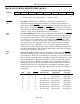
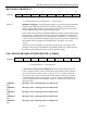
CLKOE
Bit 0
External Clock Output Enable. This bit enables the optional clock output
functions on port pin P3.5. Associated bits are shown in the following table.
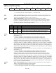
CLKOE IRDACK COD1 COD0 P3.5 Output
0 x x x General purpose I/O or T1 function
1 1 x x 16 x serial port 0 baud rate
1 0 0 0 System clock divided by 2
1 0 0 1 System clock divided by 4
1 0 1 0 System clock divided by 6
1 0 1 1 System clock divided by 8
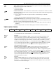
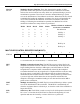
PROGRAM STATUS WORD (PSW)
7 6 5 4 3 2 1 0
SFR D0h CY AC F0 RS1 RS0 0V F1 PARITY
RW-0 RW-0 RW-0 RW-0 RW-0 RW-0 RW-0 RW-0
R = Unrestricted Read, W = Unrestricted Write, -n = Value after Reset
CY
Bit 7
Carry Flag. This bit is set when if the last arithmetic operation resulted in a carry
(during addition) or a borrow (during subtraction). Otherwise it is cleared to 0 by
all arithmetic operations.
AC
Bit 6
Auxiliary Carry Flag. This bit is set to 1 if the last arithmetic operation resulted
in a carry into (during addition), or a borrow (during subtraction) from the high
order nibble. Otherwise it is cleared to 0 by all arithmetic operations.
F0
Bit 5
User Flag 0. This is a bit-addressable, general-purpose flag for software control.
RS1, RS0
Bits 4-3
Register Bank Select 1–0. These bits select which register bank is addressed
during register accesses.
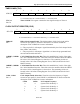
RS1 RS0 REGISTER BANK ADDRESS
0 0 0 00h – 07h
0 1 1 08h – 0Fh
1 0 2 10h – 17h
1 1 3 18h – 1Fh
OV
Bit 2
Overflow Flag. This bit is set to 1 if the last arithmetic operation resulted in a
carry (addition), borrow (subtraction), or overflow (multiply or divide).
Otherwise it is cleared to 0 by all arithmetic operations.
F1
Bit 1
User Flag 1. This is a bit-addressable, general-purpose flag for software control.
PARITY
Bit 0
Parity Flag. This bit is set to 1 if the modulo-2 sum of the eight bits of the
accumulator is 1 (odd parity); and cleared to 0 on even parity.