
Users Guide: DS80C390 Supplement Manual


High-Speed Microcontroller User’s Guide: DS80C390 Supplement
6 of 158
ADDENDUM TO SECTION 4: PROGRAMMING MODEL
The DS80C390 microprocessor is based on the industry standard 80C52. The core is an accumulator-
based architecture using internal registers for data storage and peripheral control. It executes the standard
8051 instruction set. This section provides a brief description of each architecture feature. Details
concerning the programming model, instruction set, and register description are provided in Section 4.
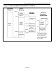
The high-speed microcontroller uses several distinct memory areas. These are registers, program
memory, and data memory. Registers serve to control on-chip peripherals and as RAM. Note that
registers (on-chip RAM) are separate from data memory. Registers are divided into three categories
including directly addressed on-chip RAM, indirectly addressed on-chip RAM, and Special Function
Registers. The program and data memory areas are discussed under Memory Map. The Registers are
discussed under Registers Map.
MEMORY MAP
The DS80C390 microprocessor uses a memory addressing scheme that separates program memory
(ROM) from data memory (RAM). Each area is accessed by a 20-bit address bus and four chip enables,
allowing a maximum address space of 4MB of program memory and 4MB of data memory. The program
and data segments can overlap since they are accessed in different ways. Program memory is fetched by
the microprocessor automatically. These addresses are never written by software. There is one instruction
(MOVC) that is used to explicitly read the program area. This is commonly used to read lookup tables.
The data memory area is accessed explicitly using the MOVX instruction. This instruction provides
multiple ways of specifying the target address.
REGISTER MAP
The register map is separate from the program and data memory areas mentioned above. A separate class
of instructions is used to access the registers. There are 256 potential register location values. In
practice, the high-speed microcontroller has 256 bytes of Scratchpad RAM and up to 128 Special
Function Registers (SFRs). This is possible since the upper 128 Scratchpad RAM locations can only be
accessed indirectly. That is, the contents of a Working Register (described below) will designate the
RAM location. Thus a direct reference to one of the upper 128 locations must be an SFR access. Direct
RAM is reached at locations 0 to 7Fh (0 to 127). SFRs are accessed directly between 80h and FFh (128
to 255). The RAM locations between 128 and 255 can be reached through an indirect reference to those
locations.
Scratchpad RAM is available for general-purpose data storage. It is commonly used in place of off-chip
RAM when the total data contents are small. When off-chip RAM is needed, the Scratchpad area will still
provide the fastest general-purpose access. Within the 256 bytes of RAM, there are several special
purpose areas. These are described as follows:
BIT ADDRESSABLE LOCATIONS
In addition to direct register access, some individual bits in both the RAM and SFR area are also
accessible. In the Scratchpad RAM area, registers 20h to 2Fh are bit addressable. This provides 126 (16 *
8) individual bits available to software. The type of instruction distinguishes a bit access from a full
register access. In the SFR area, any register location ending in a 0 or 8 is bit addressable.
WORKING REGISTERS
As part of the lower 128 bytes of RAM, there are four banks of general-purpose Working Registers, each
bank containing registers R0 through R7. The bank is selected by bits in the Program Status Word