
Users Guide: DS80C390 Supplement Manual

High-Speed Microcontroller User’s Guide: DS80C390 Supplement
35 of 158
External Connection bit (SP1EC, P5CNT.5) configures this pin as the Serial
Port 1 receive signal, disabling the corresponding CAN 1 function.
C0RX
Bit 1
CAN 0 Receive. This pin is connected to the receive data output pin of the
CAN 0 transceiver device.
C0TX
Bit 0
CAN 0 Transmit. This pin is connected to the transmit data input pin of the
CAN 0 transceiver device.
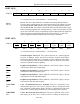
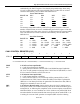
PORT 5 CONTROL REGISTER (P5CNT)
7 6 5 4 3 2 1 0
SFR A2h CAN1BA CAN0BA SP1EC C1_I/O C0_I/O P5CNT.2 P5CNT.1 P5CNT.0
RW-0 RW-0 RW-0 RW-0 RW-0 RT-0 RT-0 RT-0
R = Unrestricted Read, W =Unrestricted Write, T = Timed Access Write Only, -n = Value after Reset
CAN1BA
Bit 7
CAN 1 Bus Active. The CAN1BA signal is a latched status bit that will be set if
the respective CAN1 I/O Enabled (P5CNT.4) bit is set and bus activity detected
on the CAN 1 bus. Once activity is detected and the bit is set, it will remain set
until cleared by application software or a reset.
CAN0BA
Bit 6
CAN 0 Bus Active. The CAN0BA signal is a latched status bit that will be set if
the respective CAN0 I/O Enabled (P5CNT.3) bit is set and bus activity detected
on the CAN 0 bus. Once activity is detected and the bit is set, it will remain set
until cleared by application software or a reset.
SP1EC
Bit 5
Serial Port 1 External Connections. This bit controls whether the Serial Port 1
signals are asserted on P1.2/P1.3 or P5.2/P5.3. Rerouting the serial port signals to
Port 5 allows the use of both serial ports (but with the loss of the CAN 1 interface)
when Port 1 becomes a dedicated address bus during demultiplexed addressing
mode. Note that the corresponding port pins must be set to 1 before they can be
used in their serial port or CAN functions.
0 = Serial Port 1 signals are routed to P1.2/P1.3.
Conditions:
MUX =0, SFR bit P1.2 =1, SFR bit P1.3 =1
1 = Serial Port 1 signals are routed to P5.2/P5.3
Conditions:
MUX =0, SFR bit P5.2 =1, SFR bit P5.3 =1
C1_I/O
Bit 4
CAN 1 I/O Enable. This bit controls the function of port pins P5.2 and P5.3.
0 = Port pins P5.2 and P5.3 function as general-purpose I/O pins. The alternate
Serial Port 1 transmit and receive functions on Port 5 are only possible when this
bit is cleared to 0.
1 = Port pins P5.2 and P5.3 are dedicated to the CAN 1 receive and transmit
functions.
C0_I/O
Bit 3
CAN 0 I/O Enable. This bit controls the function of port pins P5.0 and P5.1.
0 = Port pins P5.0 and P5.1 function as general-purpose I/O pins.
1 = Port pins P5.0 and P5.1 are dedicated to the CAN 0 receive and transmit
functions.
P5CNT.2–
P5CNT.0
Port Pin P5.7-P5.4 Configuration Control Bits. These bits, in conjunction with
the P4CNT register, control which Port 5 pins (if any) are used for PCEx
decoding as shown in the table below. The memory range addressable by each
PCEx signal is a function of the total number of address lines (A19-A16)