
Users Guide: DS80C390 Supplement Manual

High-Speed Microcontroller User’s Guide: DS80C390 Supplement
25 of 158
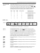
110 I/O A18 A17 A16 512 kbytes
111 A19 A18 A17 A16 1 Mbytes
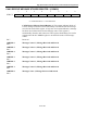
P4CNT.2-
P4CNT.0
Port Pin P4.3-P4.0 Configuration Control Bits. P4CNT.2-0 determine whether
specific P4 pins function as program chip enable signals or I/O. The memory ranges
for each
CEx signal are determined by P4CNT.5-3. Note that when the appropriate
PDCEx bit (MCON.3-0) is set, the corresponding
CEx pin will function as a
combined program/peripheral chip enable, and the respective
3PCE0PCE − will be
disabled.
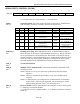
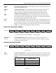
Port 4 Pin Function
P4CNT.2-0 P4.3 P4.2 P4.1 P4.0
000 I/O I/O I/O I/O
100 I/O I/O I/O
CE0
101 I/O I/O
CE1 CE0
110 I/O
CE2 CE1 CE0
111
CE3 CE2 CE1 CE0
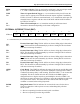
DATA POINTER EXTENDED REGISTER 0 (DPX)
7 6 5 4 3 2 1 0
SFR 93h
RW-0 RW-0 RW-0 RW-0 RW-0 RW-0 RW-0 RW-0
R = Unrestricted Read, W = Unrestricted Write, -n = Value after Reset
DPL.7-0
Bits 7-0
Data Pointer Extended Register 0. This register contains the high-order byte of
the 22-bit address (or 23-bit address when CMA=1) when performing operations
with Data Pointer 0. This register is ignored when addressing data memory in the
16-bit addressing mode.
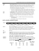
DATA POINTER EXTENDED REGISTER 1 (DPX1)
7 6 5 4 3 2 1 0
SFR 95h
RW-0 RW-0 RW-0 RW-0 RW-0 RW-0 RW-0 RW-0
R = Unrestricted Read, W = Unrestricted Write, -n = Value after Reset
DPX.7-0
Bits 7-0
Data Pointer Extended Register 1. This register contains the high-order byte of
the 22-bit address (or 23-bit address when CMA=1) when performing operations
with Data Pointer 1. This register is ignored when addressing data memory in the
16-bit addressing mode.