
Datasheet


DS89C430/DS89C450 Ultra-High-Speed Flash Microcontrollers
16 of 46
All standard SFR locations from the 8051 are duplicated in the DS89C430, and several SFRs have been added for
the unique features of the DS89C430. Most of these features are controlled by bits in SFRs located in unused
locations in the 8051 SFR map, allowing for increased functionality while maintaining complete instruction set
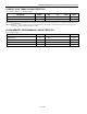
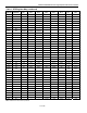
compatibility. Table 1
shows the SFRs and their locations. Table 2 specifies the default reset condition for all SFR
bits.
Data Pointers
The data pointers (DPTR and DPTR1) are used to assign a memory address for the MOVX instructions. This
address can point to a MOVX RAM location (on-chip or off-chip) or a memory-mapped peripheral. Two pointers are
useful when moving data from one memory area to another, or when using a memory-mapped peripheral for both
source and destination addresses. The user can select the active pointer through a dedicated SFR bit (SEL =
DPS.0), or can activate an automatic toggling feature for altering the pointer selection (TSL = DPS.5). An additional
feature, if selected, provides automatic incrementing or decrementing of the current DPTR.
Stack Pointer
The stack pointer denotes the register location at the top of the stack, which is the last used value. The user can
place the stack anywhere in the scratchpad RAM by setting the stack pointer to the desired location, although the
lower bytes are normally used for working registers.
I/O Ports
The DS89C430 offers four 8-bit I/O ports. Each I/O port is represented by an SFR location and can be written or
read. The I/O port has a latch that contains the value written by software.
Counter/Timers
Three 16-bit timer/counters are available in the DS89C430. Each timer is contained in two SFR locations that can
be read or written by software. The timers are controlled by other SFRs, described in the SFR Bit Description
section of the Ultra-High-Speed Flash Microcontroller User’s Guide.
Serial Ports
The DS89C430 provides two UARTs that are controlled and accessed by SFRs. Each UART has an address that
is used to read and write the value contained in the UART. The same address is used for both read and write
operations, and the read and write operations are distinguished by the instruction. Its own SFR control register
controls each UART.
Table 1. SFR Register Map
REGISTER ADDRESS BIT 7 BIT 6 BIT 5 BIT 4 BIT 3 BIT 2 BIT 1 BIT 0
P0 80h P0.7 P0.6 P0.5 P0.4 P0.3 P0.2 P0.1 P0.0
SP 81h
DPL 82h
DPH 83h
DPL1 84h
DPH1 85h
DPS 86h ID1 ID0 TSL AID — — — SEL
PCON 87h SMOD_0 SMOD0 OFDF OFDE GF1 GF0 STOP IDLE
TCON 88h TF1 TR1 TF0 TR0 IE1 IT1 IE0 IT0
TMOD 89h GATE C/T M1 M0 GATE C/T M1 M0
TL0 8Ah
TL1 8Bh
TH0 8Ch