
Datasheet


DS87C530/DS83C530 EPROM/ROM Microcontrollers with Real-Time Clock
6 of 45
PIN DESCRIPTION (continued)
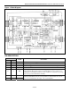
PIN
PLCC TQFP
NAME FUNCTION
30 23 P2.0 (AD8)
31 24 P2.1 (AD9)
32 25 P2.2 (AD10)
33 26 P2.3 (AD11)
34 27 P2.4 (AD12)
35 28 P2.5 (AD13)
36 29 P2.6 (AD14)
37 30 P2.7 (AD15)
Port 2 (A8–A15), I/O. Port 2 is a bidirectional I/O port. The reset condition of
Port 2 is logic high. In this state, a weak pullup holds the port high. This condition
also serves as an input mode, since any external circuit that writes to the port will
overcome the weak pullup. When software writes a 0 to any port pin, the device
will activate a strong pulldown that remains on until either a 1 is written or a reset
occurs. Writing a 1 after the port has been at 0 will cause a strong transition driver
to turn on, followed by a weaker sustaining pullup. Once the momentary strong
driver turns off, the port again becomes both the output high and input state. As an
alternate function Port 2 can function as MSB of the external address bus. This
bus can be used to read external ROM and read/write external RAM memory or
peripherals.
15 8 P3.0
16 9 P3.1
17 10 P3.2
18 11 P3.3
19 12 P3.4
20 13 P3.5
21 14 P3.6
22 15 P3.7
Port 3, I/O. Port 3 functions as both an 8-bit, bi-directional I/O port and an
alternate functional interface for external interrupts, Serial Port 0, Timer 0 and 1
Inputs, and RD and WR strobes. The reset condition of Port 3 is with all bits at a
logic 1. In this state, a weak pullup holds the port high. This condition also serves
as an input mode, since any external circuit that writes to the port will overcome
the weak pullup. When software writes a 0 to any port pin, the device will activate
a strong pulldown that remains on until either a 1 is written or a reset occurs.
Writing a 1 after the port has been at 0 will cause a strong transition driver to turn
on, followed by a weaker sustaining pullup. Once the momentary strong driver
turns off, the port again becomes both the output high and input state. The
alternate modes of Port 3 are outlined below.
Port Alternate Function
P3.0 RXD0 Serial Port 0 Input
P3.1 TXD0 Serial Port 0 Output
P3.2 INT0 External Interrupt 0
P3.3 INT1 External Interrupt 1
P3.4 T0 Timer 0 External Input
P3.5 T1 Timer 1 External Input
P3.6 WR External Data Memory Write Strobe
P3.7 RD External Data Memory Read Strobe
42 35
EA
External Access Input, Active Low. Connect to ground to use an external ROM.
Internal RAM is still accessible as determined by register settings. Connect to V
CC
to use internal ROM.
51 44 V
BAT
V
BAT
Input. Connect to the power source that maintains SRAM and RTC when
V
CC
< V
BAT
. Can be connected to a 3V lithium battery or a super cap. Connect to
GND if battery will not be used with device.
27 20 RTCX2
28 21 RTCX1
Timekeeping Crystals. A 32.768kHz crystal between these pins supplies the time
base for the RTC. The devices support both 6pF and 12.5pF load capacitance
crystals as selected by an SFR bit (described later). To prevent noise from
affecting the RTC, the RTCX2 and RTCX1 pins should be guard-ringed with
GND2.
2, 11, 13,
14, 40,
41
4, 6, 7,
33, 34,
47
N.C.
Not Connected. These pins should not be connected. They are reserved for use
with future devices in the family.