
Datasheet


DS8007
Multiprotocol Dual Smart Card Interface
2 _______________________________________________________________________________________
ABSOLUTE MAXIMUM RATINGS
ELECTRICAL CHARACTERISTICS
(V
DD
= +3.3V, V
DDA
= +3.3V, T
A
= +25°C, unless otherwise noted.) (Note 1)
Stresses beyond those listed under “Absolute Maximum Ratings” may cause permanent damage to the device. These are stress ratings only, and functional
operation of the device at these or any other conditions beyond those indicated in the operational sections of the specifications is not implied. Exposure to
absolute maximum rating conditions for extended periods may affect device reliability.
Voltage Range on V
DD
Relative to Ground ...........-0.5V to +6.5V
Voltage Range on V
DDA
Relative to Ground .........-0.5V to +6.5V
Voltage Range on Any Pin Relative to Ground
Pins CPA1, CPA2, CPB1, CPB2, and V
UP
.........-0.5V to +7.5V
All Other Pins...........................................-0.5V to (V
DD
+ 0.5V)
Maximum Junction Temperature .....................................+150°C
Continuous Power Dissipation (T
A
= +70°C)
LQFP Multilayer Board
(derate 22mW/°C above +70°C).................................1782mW
Operating Temperature Range ...........................-40°C to +85°C
Storage Temperature Range .............................-65°C to +150°C
Lead Temperature (soldering, 10s) .................................+300°C
Soldering Temperature (reflow) .......................................+260°C
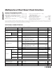
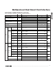
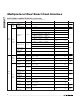
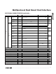
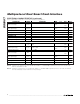
PARAMETER SYMBOL CONDITIONS MIN TYP MAX UNITS
Digital Supply Voltage V
DD
2.7 6.0 V
Step-Up Converter Supply
Voltage
V
DDA
V
DD
6.0 V
Cards Inactive f
XTAL
= 0MHz 0.9
Power-Down
V
DD
Current
Cards Active
I
PD
f
XTAL
= 0MHz, f
CLK
= 0MHz, V
CCx
= 5V 2.2
mA
Sleep Mode V
DD
Current
(Cards Active)
I
STOP
f
CLK
= 0MHz, V
CCx
= 5V 24 mA
Active V
DD
Current
5V Cards
I
DD
3x V
DD
step-up:
I
CCA
+ I
CCB
= 80mA, V
DD
= 2.7V,
f
XTAL
= 20MHz, f
CLK
= 10MHz
325 mA
2x V
DD
step-up:
I
CCA
+ I
CCB
= 80mA, f
XTAL
= 20MHz,
f
CLK
= 10MHz, V
DD
= 2.7V
225
Active V
DD
Current
3V Cards
I
DD
No step-up:
I
CCA
+ I
CCB
= 80mA, f
XTAL
= 20MHz,
f
CLK
= 10MHz, V
DD
= 5V
120
mA
V
RST
Threshold voltage (falling) 2.1 2.5 V
Power-Fail Reset Voltage
V
HYS
Hysteresis 50 170 mV
Reset
Threshold
V
DRST
1.25
Output Voltage V
DO
V
DD
+
0.3
V
V
DELAY
= 0V -2 μA
Output Current I
DO
V
DELAY
= V
DD
+2 mA
Delay Pin
Output
Capacitance
C
DO
1 nF
RSTOUT PIN
Output High Voltage V
OHRSTO
I
OH
= -1mA
0.8 x
V
DD
V
DD
+
0.3
V
Output Low Voltage V
OLRSTO
I
OL
= 2mA -0.3 +0.4 V
Leakage Current I
L
V
OL
= 0V, V
OH
= 5V -10 +10 μA