
User guide

DS4830A User’s Guide
67
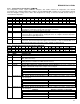
channels and hence their ADC conversion will be delayed. When the FAST_MODE bit is set to ‘0’, the user can
issue SHEN pulse every 250µs time interval.
Note: When averaging is used for ADC channels or S/H’s, the S/H conversion time slot changes as shown in Figure
7-5 and cannot be guaranteed to get conversion slot in 125µs or 250µs. The S/H conversion time depends upon
number of ADC samples to be averaged.
8.1.3 – Sampling Control
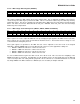
The sample and hold circuitry provides the option to select the internal peripheral clock or the external clock. When
the clock select bit CLK_SEL (located in the SHCN register) is set to ‘0’, the peripheral clock is used for the sample
and hold circuit. When the clock select bit CLK_SEL is set to ‘1’, the external clock (CLKIN on the DACPW2 pin) is
used for the sample and hold circuit.
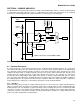
Sample
Pulse
External
Trigger
Internal
Trigger
0
1
Mux
INTTRIG
_EN
0
Non
-
Zero
Mux
SSC
SHEN OUT
{
SHEN OUT when SSC
=
0
Sampling Pulse depends
upon SSC Value
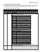
Figure 8-3: Sample Pulse
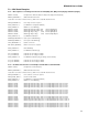
The end of the sample and hold sample time is controlled by the Sampling Stop Control bits SSC[3:0] in the SHCN
register. These bits are used along with the CLK_SEL bit to determine the length of the sample pulse. When the
SSC[3:0] bits have non-zero values and the CLK_SEL bit is set to ‘1’, the stop sampling depends upon the number
of external clock cycles. When the SSC[3:0] bits have non-zero values and the CLK_SEL bit is ‘0’, the stop sampling
depends upon the time from the rising edge of SHEN0/1 (See Figure 8-3 for Sample Pulse). See SSC[3:0] bit
description for stop sampling timings.
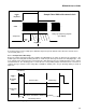
Falling edge (Sample stop) depends
upon SSC[3:0]
SHEN0/1
or
INT_REIG0/1
Sample
Pulse
Sample Pulse Width with peripheral clock
300ns
min
SSC[3:0] = 0
Figure 8-4: Sample Pulse Width with the Peripheral Clock
As shown in Figure 8-4, the sample pulse width time depends upon the SSC bits value when the peripheral clock is
selected (CLK_SEL = 0).