
User guide


DS4830A User’s Guide
173
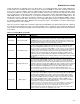
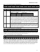
Table 21-4: Output from Read Register Map Command
WO
RD
REGISTER
WO
RD
REGISTER
WO
RD
REGISTER WORD REGISTER WORD REGISTER WORD REGISTER
WO
RD
REGISTER
0 PO2 32
64
96 MCNT 128 ADCN 160
192 A[3]
1 PO1 33 I2CST_M 65 I2CST_S 97 MA 129 SENR 161 QTCN 193 A[4]
2 PO0 34 I2CIE_M 66 MPNTR 98 MB 130 ADST 162 LTIL 194 A[5]
3 EIF2 35 PO6 67 I2CTXFST 99 MC2 131 ADST1 163 HTIL 195 A6[]
4 EIF1 36 CRC8IN 68 I2CTXFIE 100 MC1 132
164
196 A[7]
5 EIF0 37 MIIR1 69 I2CRXFST 101 MC0 133
165
197 A[8]
6 GTV1 38 EIF6 70 I2CRXFIE 102 GTCN2 134 DADDR 166 PWMCN 198 A[9]
7 GTCN1 39 EIE6 71 I2CST2_S 103 SHFT 135 MIIR4 167 PWMSYNC 199 A[10]
8 PI2 40 PI6 72 RPNTR 104 MC1R 136 TEMPCN 168 LTIH 200 A[11]
9 PI1 41 SVM 73
105 MC0R 137 SHCN 169 HTIH 201 A[12]
10 PI0 42 - 74
106 GTC2 138 ADMIS 170 QTLST 202 A[13]
11 GTC1 43 - 75
107 GTV2 139 PINSEL 171
203 A[14]
12 44 I2CCN_M 76 I2CSLA_S 108 GR_REG1 140 REFAVG 172
204 A[15]
13 EIE2 45 I2CCK_M 77 I2CSLA2_S 109 GR_REG2 141
173
205 IP
14 EIE1 46 I2CTO_M 78 I2CSLA3_S 110 MACRSEL 142 TWR 174 MIIR5 206 SP
15 EIE0 47 I2CSLA_M 79 I2CSLA4_S 111 USER_INT 143 RPCFG 175
207 IV
16 PD2 48 EIES6 80 I2CIE2_S 112 GR_REG3 144 SPICN_S 176
208 LC[0]
17 PD1 49 PD6 81 MADDR 113 GR_REG4 145 SPICF_S 177
209 LC[1]
18 PD0 50
82 MADDR2 114 GR_REG5 146 SPICK_S 178 SPICN_M 210 OFFS
19 EIES2 51
83 MADDR3 115 GR_REG6 147 I2C_SPB 179 SPICF_M 211 DPC
20 EIES1 52
84 MADDR4 116 GR_REG7 148 DEV_NUM 180 SPICK_M 212 GR
21 EIES0 53 CRC8OUT 85 CUR_SLA 117 GR_REG8 149 DACD0 181
213 BP
22 54
86 I2CIE_S 118 GR_REG9
150 DACD1 182
214 DP[0]
23 55 ADCG1 87 119 GR_REG10 151 DACD2 183
215 DP[1]
24 56 ADCG2 88 ICDT0 120 GR_REG11 152 DACD3 184 AP APC
25 57 ADVOFF 89 ICDT1 121 GR_REG12 153 DACD4 185 PSF IC
26 58
90 ICDC 122 GR_REG13 154 DACD5 186 IMR SC
27 59 ADCG3 91 ICDF 123 GR_REG14 155 DACD6 187 IIR CKCN
28 60 ADCG4 92 ICDB 124 GR_REG15 156 DACD7 188 WDCN 0
29 61 CHIPREV 93 ICDA 125 GR_REG16 157 DACCFG 189 A[0]
30 62 ICSLA2_M 94 ICDD 126 158 ADADDR 190 A[1]
31 63 95 127 159
191 A[2]
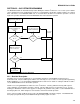
21.2.3 – Single Step Operation (Trace)
The debug engine supports single step operation in debug mode by executing a Trace command from the host. The
debug engine allows the CPU to return to its normal program execution for one cycle and then forces a debug mode
re-entry. The steps for the Trace command are:
1) Set status to 10b (debug-busy)
2) Pop the return address from the stack
3) Set the IGE bit to logic 1 if debug mode was activated when IGE=1.
4) Supply the CPU with an instruction addressed by the return address
5) Stall the CPU at the end of the instruction execution
6) Block the next instruction fetch from program memory
7) Push the return address onto the stack
8) Set the contents of IP to x8010h
9) Clear the IGE bit to 0 to disable the interrupt handler
10) Halt CPU operation
11) Set the status to debug-idle
Note that the trace operation uses a return address from the stack as a legitimate address for program fetching. The
host must maintain consistency of program flow during the debug process. The Instruction Pointer is automatically
incremented after each trace operation, thus a new return address will be pushed onto the stack before returning the
control to the debug engine. Also, note that the interrupt handler is an essential part of the CPU and a pending
interrupt could be granted during single step operation since the IGE bit state present on debug mode entry is
restored for the single step.