
Datasheet


Extremely Accurate I
2
C RTC with
Integrated Crystal and SRAM
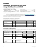
Data Transfer on I
2
C Serial Bus
SCL
NOTE: TIMING IS REFERENCED TO V
IL(MAX)
AND V
IH(MIN)
.
SDA
STOP START REPEATED
START
t
BUF
t
HD:STA
t
HD:DAT
t
SU:DAT
t
SU:STO
t
HD:STA
t
SP
t
SU:STA
t
HIGH
t
R
t
F
t
LOW
Note 2: Limits at -40°C are guaranteed by design and not production tested.
Note 3: All voltages are referenced to ground.
Note 4: I
CCA
—SCL clocking at max frequency = 400kHz.
Note 5: Current is the averaged input current, which includes the temperature conversion current.
Note 6: The RST pin has an internal 50kΩ (nominal) pullup resistor to V
CC
.
Note 7: After this period, the first clock pulse is generated.
Note 8: A device must internally provide a hold time of at least 300ns for the SDA signal (referred to the V
IH(MIN)
of the SCL signal)
to bridge the undefined region of the falling edge of SCL.
Note 9: The maximum t
HD:DAT
needs only to be met if the device does not stretch the low period (t
LOW
) of the SCL signal.
Note 10: A fast-mode device can be used in a standard-mode system, but the requirement t
SU:DAT
≥ 250ns must then be met. This
is automatically the case if the device does not stretch the low period of the SCL signal. If such a device does stretch the
low period of the SCL signal, it must output the next data bit to the SDA line t
R(MAX)
+
t
SU:DAT
= 1000 + 250 = 1250ns
before the SCL line is released.
Note 11: C
B
—total capacitance of one bus line in pF.
Note 12: Minimum operating frequency of the I
2
C interface is imposed by the timeout period.
Note 13: The parameter t
OSF
is the period of time the oscillator must be stopped for the OSF flag to be set over the voltage range of
0V ≤ V
CC
≤ V
CC(MAX)
and 2.3V ≤ V
BAT
≤ 3.4V.
Note 14: This delay only applies if the oscillator is enabled and running. If the EOSC bit is 1, t
REC
is bypassed and RST immediately
goes high.
WARNING: Negative undershoots below -0.3V while the part is in battery-backed mode may
cause loss of data.
DS3232
6
Maxim Integrated