
Datasheet


event, it is possible that the microcontroller and DS3232
I
2
C communications could become unsynchronized,
e.g., the microcontroller resets while reading data from
the DS3232. When the microcontroller resets, the
DS3232 I
2
C interface may be placed into a known state
by toggling SCL until SDA is observed to be at a high
level. At that point the microcontroller should pull SDA
low while SCL is high, generating a START condition.
If SCL is held low for greater than t
IF
, the internal I
2
C
interface is reset. This limits the minimum frequency at
which the I
2
C interface can be operated. If data is
being written to the device when the interface timeout is
exceeded, prior to the acknowledge, the incomplete
byte of data is not written.
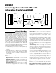
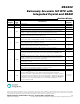
Clock and Calendar
The time and calendar information is obtained by read-
ing the appropriate register bytes. Figure 1 illustrates
the RTC registers. The time and calendar data are set
or initialized by writing the appropriate register bytes.
The contents of the time and calendar registers are in
binary-coded decimal (BCD) format. The DS3232 can
be run in either 12-hour or 24-hour mode. Bit 6 of the
Extremely Accurate I
2
C RTC with
Integrated Crystal and SRAM
Figure 1. Address Map for DS3232 Timekeeping Registers and SRAM
Note: Unless otherwise specified, the registers’ state is not defined when power is first applied.
ADDRESS
BIT 7
MSB
BIT 6 BIT 5 BIT 4 BIT 3 BIT 2 BIT 1
BIT 0
LSB
FUNCTION RANGE
00h 0 10 Seconds Seconds Seconds 00–59
01h 0 10 Minutes Minutes Minutes 00–59
AM/PM
02h 0 12/24
20 Hour
10 Hour Hour Hours
1–12 + AM/PM
00–23
03h 0 0 0 0 0 Day Day 1–7
04h 0 0 10 Date Date Date 1–31
05h Century 0 0 10 Month Month
Month/
Century
01–12 +
Century
06h 10 Year Year Year 00–99
07h A1M1 10 Seconds Seconds Alarm 1 Seconds 00–59
08h A1M2 10 Minutes Minutes Alarm 1 Minutes 00–59
AM/PM
09h A1M3 12/24
20 Hour
10 Hour Hour Alarm 1 Hours
1–12 + AM/PM
00–23
Day Alarm 1 Day 1–7
0Ah A1M4 DY/DT 10 Date
Date Alarm 1 Date 1–31
0Bh A2M2 10 Minutes Minutes Alarm 2 Minutes 00–59
AM/PM
0Ch A2M3 12/24
20 Hour
10 Hour Hour Alarm 2 Hours
1–12 + AM/PM
00–23
Day Alarm 2 Day 1–7
0Dh A2M4 DY/DT 10 Date
Date Alarm 2 Date 1–31
0Eh EOSC BBSQW CONV RS2 RS1 INTCN A2IE A1IE Control —
0Fh OSF BB32kH zC RATE 1 CRATE0 EN32kHz BSY A2F A1F Control/Status —
10h SIGN DATA DATA DATA DATA DATA DATA DATA Aging Offset —
11h SIGN DATA DATA DATA DATA DATA DATA DATA MSB of Temp —
12h DATA DATA 0 0 0 0 0 0 LSB of Temp —
13h 0 0 0 0 0 0 0 0 Not used
Reserved for
test
14h–0FFh x x x x x x x x SRAM 00h–0FFh
DS3232
Maxim Integrated
11