
Datasheet
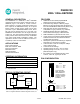


DS28EC20: 20Kb 1-Wire EEPROM
5 of 27
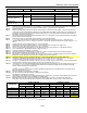
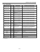
Note 1:
System requirement.
Note 2:
Maximum allowable pullup resistance is a function of the number of 1-Wire devices in the system, 1-Wire recovery times, and
current requirements during EEPROM programming. The specified value here applies to systems with only one device and with
the minimum 1-Wire recovery times. For more heavily loaded systems, an active pullup such as that found in the DS2482-x00,
DS2480B, or DS2490 may be required.
Note 3:
Typical value represents the internal parasite capacitance when V
PUP
is first applied. Once the parasite capacitance is charged, it
does not affect normal communication.
Note 4:
Guaranteed by design, characterization and/or simulation only. Not production tested.
Note 5:
V
TL
, V
TH
, and V
HY
are a function of the internal supply voltage which is itself a function of V
PUP
, R
PUP
, 1-Wire timing, and
capacitive loading on I/O. Lower V
PUP
, higher R
PUP
, shorter t
REC
, and heavier capacitive loading all lead to lower values of V
TL
, V
TH
,
and V
HY
.
Note 6:
Voltage below which, during a falling edge on I/O, a logic 0 is detected.
Note 7:
The voltage on I/O needs to be less or equal to V
ILMAX
at all times the master is driving I/O to a logic 0 level.
Note 8:
Voltage above which, during a rising edge on I/O, a logic 1 is detected.
Note 9:
After V
TH
is crossed during a rising edge on I/O, the voltage on I/O has to drop by at least V
HY
to be detected as logic 0.
Note 10:
The I-V characteristic is approximately linear for voltages less than 1V.
Note 11:
Applies to a single device attached to a 1-Wire line.
Note 12:
The earliest recognition of a negative edge is possible at t
REH
after V
TH
has been reached on the preceding rising edge.
Note 13:
Defines maximum possible bit rate. Equal to 1/(t
W0LMIN
+ t
RECMIN
).
Note 14:
Interval after t
RSTL
during which a bus master can read a logic 0 on I/O if there is a DS28EC20 present. The power-up presence
detect pulse could be outside this interval but will be complete within 2ms after power-up.
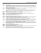
Note 15:
ε in Figure 11 represents the time required for the pullup circuitry to pull the voltage on I/O up from V
IL
to V
TH
. The actual
maximum duration for the master to pull the line low is t
W1LMAX
+ t
F
- ε and t
W0LMAX
+ t
F
- ε, respectively.
Note 16:
δ in Figure 11 represents the time required for the pullup circuitry to pull the voltage on I/O up from V
IL
to the input high threshold
of the bus master. The actual maximum duration for the master to pull the line low is t
RLMAX
+ t
F
.
Note 17:
Current drawn from I/O during the EEPROM programming interval. The pullup circuit on I/O during the programming interval
should be such that the voltage at I/O is greater than or equal to 3.0V. For 3.3V±5% V
PUP
operation of the DS28EC20, a low-
impedance bypass of R
PUP
, which can be activated during programming, is required.
Note 18:
The t
PROG
interval begins t
REHMAX
after the trailing rising edge on I/O for the last time slot of the E/S byte for a valid copy scratchpad
sequence. Interval ends once the device's self-timed EEPROM programming cycle is complete and the current drawn by the
device has returned from I
PROG
to I
L
.
Note 19:
Write-cycle endurance is degraded as T
A
increases.
Note 20:
Not 100% production-tested; guaranteed by reliability monitor sampling.
Note 21:
Data retention is degraded as T
A
increases.
Note 22:
Guaranteed by 100% production test at elevated temperature for a shorter time; equivalence of this production test to data sheet
limit at operating temperature range is established by reliability testing.
Note 23:
EEPROM writes may become nonfunctional after the data retention time is exceeded. Long-time storage at elevated
temperatures is not recommended; the device may lose its write capability after 10 years at +125°C or 40 years at +85°C.