
Datasheet


DS28E05 1-Wire EEPROM
www.maximintegrated.com
Maxim Integrated
│
4
Pin Descriptions
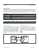
Pin Congurations
Detailed Description
TheDS28E05combines896bitsofuserEEPROMorga-
nized as seven 128-bit pages, 64 bits of administrative
datamemory,anda64-bitROMIDinasinglechip.Data
istransferredseriallythroughthe1-Wireprotocol,which
requires only a single data lead and a ground return.
The user memory can have unrestricted write access (fac-
torydefault),orcanbewriteprotectedorputinEPROM
emulation mode. Write protection prevents changes to
the memory data. EPROM emulation mode logically
ANDsmemorydatawithincomingnewdata,whichallows
changingbitsfrom1to0,butnotviceversa.Bychang-
ing one bit at a time this mode could be used to create
nonvolatile nonresettable counters. For more details
refer to ApplicationNote5042:Implementing Nonvolatile,
Nonresettable Counters for Embedded Systems.
The device’s 64-bit ROM ID can be used to electronically
identify the equipment in which the DS28E05 is used.
The ROM ID guarantees unique identification and is also
used to address the device in a multidrop 1-Wire network
environment, where multiple devices reside on a com-
mon 1-Wire bus and operate independently of each other.
Applicationsincludeaccessory/PCB identification,medi-
calsensorcalibrationdatastorage,analogsensorcalibra-
tion,andafter-marketmanagementofconsumables.
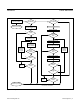
Overview
The block diagram in Figure 1 shows the relationships
between the major control and memory sections of the
DS28E05. The DS28E05 has three main data compo-
nents: seven 128-bit pages of user EEPROM, 64 bits
of administrative data memory, and a 64-bit ROM ID.
Figure 2 shows the hierarchic structure of the 1-Wire
protocol. The bus master must first provide one of the
fiveROMfunctioncommands:ReadROM,MatchROM,
Search ROM, Skip ROM, or Resume Communication.
The protocol required for these ROM function commands
is described in
Figure8.AfteraROMfunctioncommand
issuccessfullyexecuted,thememoryfunctionsbecome
accessible and the master can select one of the two
memory function commands. The function protocols are
described in
Figure6. All data is read and written least
significant bit first.
64-Bit ROM ID
Each DS28E05 contains a unique ROM ID that is 64 bits
long. The first 8 bits are a 1-Wire family code. The next
48 bits are a unique serial number. The last 8 bits are a
cyclicredundancycheck(CRC)ofthefirst56bits.See
Figure3fordetails.The1-WireCRCisgeneratedusing
a polynomial generator consisting of a shift register and
XORgatesasshowninFigure4.
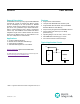
PIN
NAME FUNCTION
SOT23 TSOC
2 3–6 N.C.
NotConnected
1 2 IO 1-WireBusInterface.Open-drainsignalthatrequiresanexternalpullupresistor.
3 1 GND GroundReference
N.C.
IO
GND
N.C.
N.C.
N.C.
TSOC
TOP VIEW
+
5
4
6
2
3
1
DS28E05
DS28E05
N.C.
1
3GND
IO
+
0Drr
SOT23
TOP VIEW
2