
Datasheet


DS28E05 1-Wire EEPROM
www.maximintegrated.com
Maxim Integrated
│
3
Electrical Characteristics (continued)
(T
A
=-40°Cto+85°C,unlessotherwisenoted.)(Note1)
Note 1: Limitsare100%productiontestedatT
A
=+25°Cand/orT
A
=+85°C.Limitsovertheoperatingtemperaturerangeandrel-
evant supply voltage range are guaranteed by design and characterization. Typical values are not guaranteed.
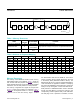
Note 2: System requirement.
Note 3: Maximum allowable pullup resistance is a function of the number of 1-Wire devices in the system and 1-Wire recovery
times. The specified value here applies to systems with only one device and with the minimum 1-Wire recovery times.
Note 4: TypicalvaluerepresentstheinternalparasitecapacitancewhenV
PUP
is first applied. Once the parasite capacitance is
charged,itdoesnotaffectnormalcommunication.
Note 5: Guaranteedbydesignand/orcharacterizationonly.Notproductiontested.
Note 6:V
TL
,V
TH
,andV
HY
areafunctionoftheinternalsupplyvoltage,whichisafunctionofV
PUP
,R
PUP
,1-Wiretiming,and
capacitiveloadingonIO.LowerV
PUP
,higherR
PUP
,shortert
REC
,andheaviercapacitiveloadingallleadtolowervaluesof
V
TL
,V
TH
,andV
HY
.
Note 7: Voltagebelowwhich,duringafallingedgeonIO,alogic0isdetected.
Note 8: ThevoltageonIOmustbelessthanorequaltoV
ILMAX
at all times the master is driving IO to a logic 0 level.
Note 9: Voltageabovewhich,duringarisingedgeonIO,alogic1isdetected.
Note 10:AfterV
TH
iscrossedduringarisingedgeonIO,thevoltageonIOmustdropbyatleastV
HY
to be detected as logic 0.
Note 11:TheI-Vcharacteristicislinearforvoltageslessthan1V.
Note 12:Appliestoasingledeviceattachedtoa1-Wireline.
Note 13:Definesmaximumpossiblebitrate.Equalto1/(t
W0LMIN
+t
RECMIN
).
Note 14:Anadditionalresetorcommunicationsequencecannotbeginuntiltheresethightimehasexpired.
Note 15: Interval after t
RSTL
during which a bus master can read a logic 0 on IO if there is a DS28E05 present. The power-up pres-
ence detect pulse could be outside this interval but will be complete within 2ms after power-up.
Note 16:εinFigure10representsthetimerequiredforthepullupcircuitrytopullthevoltageonIOupfromV
IL
toV
TH
. The actual
maximum duration for the master to pull the line low is t
W1LMAX
+t
F
-εandt
W0LMAX
+t
F
-ε,respectively.
Note 17:δinFigure10representsthetimerequiredforthepullupcircuitrytopullthevoltageonIOupfromV
IL
to the input-high
threshold of the bus master. The actual maximum duration for the master to pull the line low is t
RLMAX
+t
F
.
Note 18:CurrentdrawnfromIOduringtheEEPROMprogramminginterval,duringwhichthevoltageatIOmustnotdropbelow1.8V.
This condition is met with R
PUPMAX
overtheentireV
PUP
range.
Note 19: The t
PROG
interval begins immediately after the trailing rising edge on IO for the last time slot of the Release byte for a
valid Write Memory sequence. Interval ends once the device’s self-timed EEPROM programming cycle is complete and the
current drawn by the device has returned from I
PROG
to I
L
.
Note 20:Write-cycleenduranceistestedincompliancewithJESD47G.
Note 21:Not100%productiontested;guaranteedbyreliabilitymonitorsampling.
Note 22:DataretentionistestedincompliancewithJESD47G.
Note 23:Guaranteedby100%productiontestatelevatedtemperatureforashortertime;equivalenceofthisproductiontesttothe
data sheet limit at operating temperature range is established by reliability testing.
Note 24: EEPROM writes can become nonfunctional after the data-retention time is exceeded. Long-term storage at elevated tem-
peratures is not recommended.