
Datasheet


DS28E04-100: 4096-Bit 1-Wire Addressable EEPROM with PIO
4 of 37
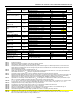
Note 19:
ε in Figure 16 represents the time required for the pullup circuitry to pull the voltage on IO up from V
IL
to V
TH
. The actual maximum
duration for the master to pull the line low is t
W1LMAX
+ t
F
- ε and t
W0LMAX
+ t
F
- ε respectively.
Note 20:
δ in Figure 16 represents the time required for the pullup circuitry to pull the voltage on IO up from V
IL
to the input high threshold
of the bus master. The actual maximum duration for the master to pull the line low is t
RLMAX
+ t
F
.
Note 21:
Current drawn during the EEPROM programming interval. If the device does not get V
CC
power, the pullup circuit on IO during the
programming interval should be such that the voltage at IO is greater than or equal to V
PUP
(min). If V
PUP
in the system is close to
Vpup(min) then a low-impedance bypass of R
PUP
that can be activated during programming may need to be added.
Note 22:
The t
PROG
interval begins t
REHmax
after the trailing rising edge on IO for the last time slot of the E/S byte for a valid Copy Scratchpad
sequence. Interval ends once the device's self-timed EEPROM programming cycle is complete and the current drawn by the
device has returned from I
PROG
to I
L
or I
CCS
, respectively.
Note 23:
Not production tested. Guaranteed by design or characterization.
Note 24:
EEPROM writes can become nonfunctional after the data-retention time is exceeded. Long-time storage at elevated temperatures
is not recommended; the device can lose its write capability after 10 years at +125°C or 40 years at +85°C.
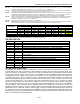
LEGACY VALUES
DS28E04-100 VALUES
PARAMETER
STANDARD SPEED
OVERDRIVE SPEED
STANDARD SPEED
OVERDRIVE SPEED
MIN
MAX
MIN
MAX
MIN
MAX
MIN
MAX
t
SLOT
(incl. t
REC
)
61µs
(undef)
7µs
(undef)
65µs
1)
(undef)
9µs
(undef)
t
RSTL
480µs
(undef)
48µs
80µs
504µs
640µs
53µs
80µs
t
PDH
15µs
60µs
2µs
6µs
15µs
60µs
2µs
7µs
t
PDL
60µs
240µs
8µs
24µs
60µs
240µs
8µs
26µs
t
W0L
60µs
120µs
6µs
16µs
60µs
120µs
7µs
16µs
1)
Intentional change, longer recovery time requirement due to modified 1-Wire front end.
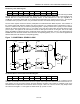
PIN DESCRIPTION
PIN
NAME
FUNCTION
1
A3
Address bit input (place value = 8), with weak pullup.
2
A2
Address bit input (place value = 4), with weak pullup.
3
A1
Address bit input (place value = 2), with weak pullup.
4
A0
Least significant address bit input (place value = 1), with weak pullup.
5, 12
GND
Ground Reference
6, 11
N.C.
Not Connected
7
V
CC
Optional power supply for the chip; leave unconnected or ground if V
CC
power
is not available.
8
POL
Power-up polarity (logical state) for P0 and P1; pin has a weak pulldown.
9
P0
Remote-controlled I/O pin, open drain with weak pulldown.
10
P1
Remote-controlled I/O pin, open drain with weak pulldown.
13
A6
Address bit input (place value = 64), with weak pullup.
14
A5
Address bit input (place value = 32), with weak pullup.
15
A4
Address bit input (place value = 16), with weak pullup.
16
IO
1-Wire Bus Interface. Open drain, requires external pullup resistor.
DETAILED DESCRIPTION
The DS28E04-100 combines 4096 bits of EEPROM, a 16-byte control page, two general-purpose PIO pins, seven
external address pins, and a fully featured 1-Wire interface in a single chip. PIO outputs are configured as open-
drain and provide an on-resistance of 100Ω max. A robust PIO channel-access communication protocol ensures
that PIO output-setting changes occur error-free. The DS28E04-100 has an additional memory area called the
scratchpad that acts as a buffer when writing to the main memory or the control page. Data is first written to the
scratchpad from which it can be read back. The copy scratchpad command transfers the data to its final memory
location. Each DS28E04-100 has a device ID number that is 64 bits long. The user can define seven bits of this
number through address pins. The remaining 57 bits are factory-lasered into the chip. The device ID number
guarantees unique identification and is used to address the device in a multidrop 1-Wire network environment,
where multiple devices reside on a common 1-Wire bus and operate independently of each other. The DS28E04-
100 also supports 1-Wire conditional search capability based on PIO conditions or power-on-reset activity. The
DS28E04-100 has an optional V
CC
supply connection. When an external supply is absent, device power is supplied
parasitically from the 1-Wire bus. When an external supply is present, PIO states are maintained in the absence of
the 1-Wire bus power source. Applications of the DS28E04-100 include autoconfiguration and state monitoring of
modular systems such as central-office switches, cellular base stations, access products, optical network units, and
PBXs, and accessory/PC board identification.