
Datasheet


DS28E04-100: 4096-Bit 1-Wire Addressable EEPROM with PIO
29 of 37
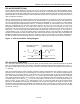
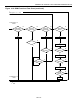
Master-to-Slave
For a write-one time slot, the voltage on the data line must have crossed the V
TH
threshold before the write-one
low time t
W 1LMAX
is expired. For a write-zero time slot, the voltage on the data line must stay below the V
TH
threshold until the write-zero low time t
W0LMIN
is expired. For the most reliable communication, the voltage on the
data line should not exceed V
ILMAX
during the entire t
W0L
or t
W1L
window. After the V
TH
threshold has been crossed,
the DS28E04-100 needs a recovery time t
REC
before it is ready for the next time slot.
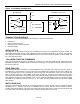
Slave-to-Master
A read-data time slot begins like a write-one time slot. The voltage on the data line must remain below V
TL
until the
read low time t
RL
is expired. During the t
RL
window, when responding with a 0, the DS28E04-100 starts pulling the
data line low; its internal timing generator determines when this pulldown ends and the voltage starts rising again.
When responding with a 1, the DS28E04-100 does not hold the data line low at all, and the voltage starts rising as
soon as t
RL
is over.
The sum of t
RL
+ δ (rise time) on one side and the internal timing generator of the DS28E04-100 on the other side
define the master sampling window (t
MSRMIN
to t
MSRMAX
) in which the master must perform a read from the data line.
For the most reliable communication, t
RL
should be as short as permissible, and the master should read close to
but no later than t
MSRMAX
. After reading from the data line, the master must wait until t
SLOT
is expired. This
guarantees sufficient recovery time t
REC
for the DS28E04-100 to get ready for the next time slot. Note that t
REC
specified herein applies only to a single DS28E04-100 attached to a 1-Wire line. For multidevice configurations,
t
REC
needs to be extended to accommodate the additional 1-Wire device input capacitance. Alternatively, an
interface that performs active pullup during the 1-Wire recovery time such as the DS2482-x00 or DS2480B 1-Wire
line drivers can be used.
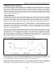
IMPROVED NETWORK BEHAVIOR (SWITCHPOINT HYSTERESIS)
In a 1-Wire environment, line termination is possible only during transients controlled by the bus master (1-Wire
driver). 1-Wire networks, therefore, are susceptible to noise of various origins. Depending on the physical size and
topology of the network, reflections from end points and branch points can add up, or cancel each other to some
extent. Such reflections are visible as glitches or ringing on the 1-Wire communication line. Noise coupled onto the
1-Wire line from external sources can also result in signal glitching. A glitch during the rising edge of a time slot can
cause a slave device to lose synchronization with the master and, consequently, result in a search ROM command
coming to a dead end or cause a device-specific function command to abort. For better performance in network
applications, the DS28E04-100 uses a new 1-Wire front end, which makes it less sensitive to noise and also
reduces the magnitude of noise injected by the slave device itself.
The 1-Wire front end of the DS28E04-100 differs from traditional slave devices in four characteristics.
1) The falling edge of the presence pulse has a controlled slew rate. This provides a better match to the line
impedance than a digitally switched transistor, converting the high-frequency ringing known from traditional
devices into a smoother low-bandwidth transition. The slew-rate control is specified by the parameter t
FPD
,
which has different values for standard and Overdrive speed.
2) There is additional lowpass filtering in the circuit that detects the falling edge at the beginning of a time slot.
This reduces the sensitivity to high-frequency noise. This additional filtering does not apply at Overdrive speed.
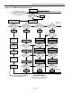
3) There is a hysteresis at the low-to-high switching threshold V
TH
. If a negative glitch crosses V
TH
but does not go
below V
TH
- V
HY
, it will not be recognized (Figure 17, Case A). The hysteresis is effective at any 1-Wire speed.
4) There is a time window specified by the rising edge hold-off time t
REH
during which glitches are ignored, even if
they extend below V
TH
- V
HY
threshold (Figure 17, Case B, t
GL
< t
REH
). Deep voltage droops or glitches that
appear late after crossing the V
TH
threshold and extend beyond the t
REH
window cannot be filtered out and are
taken as the beginning of a new time slot (Figure 17, Case C, t
GL
≥ t
REH
).
Only devices that have the parameters t
FPD
, V
HY
, and t
REH
specified in their electrical characteristics use the
improved 1-Wire front end.